

Drain Characteristics of an n-Channel MOSFET (2N7000)
Adapted from the ExpEYES blog MOSFET drain-curve lab. Sweep $V_{DS}$ with PV1 at fixed $V_{GS}$ (PV2) and plot $I_D$ vs $V_{DS}$.
1. Aim
To obtain the output (drain) characteristics of a 2N7000 MOSFET for several gate–source voltages and to identify the cutoff / linear / saturation behaviour qualitatively.
2. Apparatus / Components Required
- SEELab3 / ExpEYES-17 (PV1, PV2, A1)
- 2N7000 n-channel MOSFET
- Series drain resistor $R_D = 1\text{ k}\Omega$
- Breadboard and wires
- Python 3 with
eyes17,matplotlib(for the scripted sweep)
3. Theory & Principle
For an n-channel enhancement MOSFET, appreciable drain current appears only when $V_{GS}$ exceeds a threshold (for 2N7000, conduction in this setup is weak below about 1.65 V gate bias).
Indirect drain current (same method as diode/transistor labs):
\[I_D = \frac{V_{\text{PV1}} - V_{\text{A1}}}{R_D}, \qquad V_{DS} \approx V_{\text{A1}}\](with source grounded). Family of curves: fix $V_{GS}$ via PV2, sweep PV1, plot $I_D$ vs $V_{DS}$.
4. Circuit Diagram / Setup
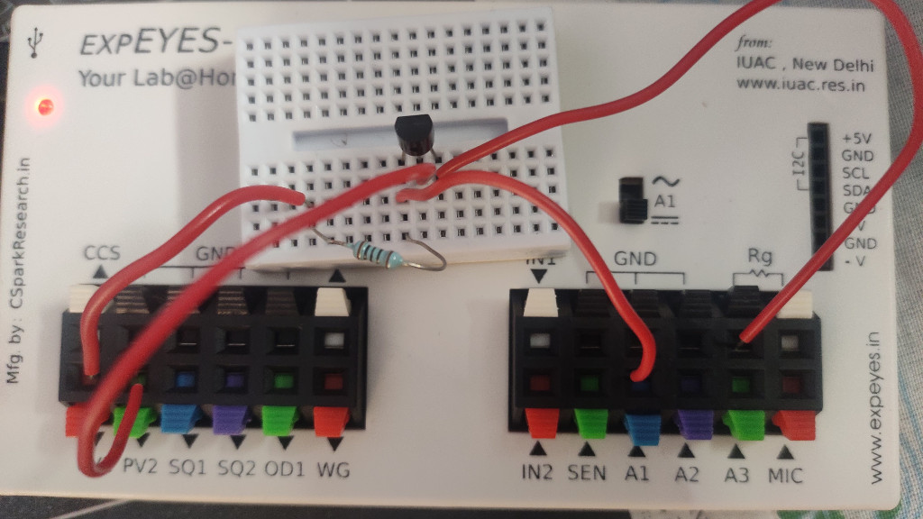
- Source → GND.
- Gate → PV2.
- PV1 → $R_D = 1\text{ k}\Omega$ → Drain.
- A1 at the drain node ($V_{DS}$).
5. Procedure
Part A — App / manual observation
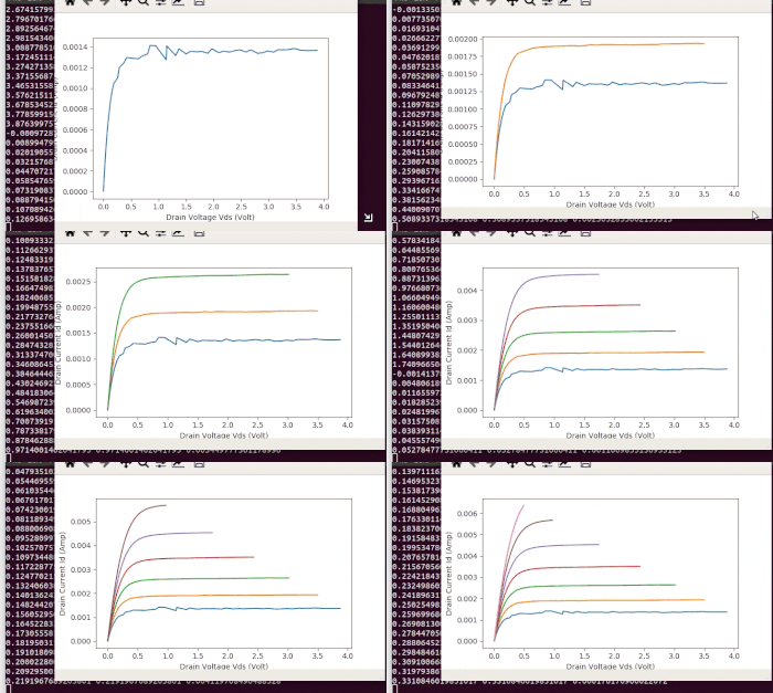
- Set PV2 to a fixed gate voltage (start near 1.7 V).
- Sweep PV1 from 0 toward ~5 V; record A1 and compute $I_D$.
- Repeat for several PV2 values up to about 2.0 V.
- Plot $I_D$ vs $V_{DS}$ for each $V_{GS}$.
Part B — Python automation
1
2
3
4
5
6
7
8
9
10
11
12
13
14
15
16
17
18
19
20
21
22
23
24
25
26
27
28
29
30
31
import time
import eyes17.eyes
from pylab import *

p = eyes17.eyes.open()
xlabel("Drain voltage V_DS (V)")
ylabel("Drain current I_D (A)")
ion()

pv2 = 1.65
while pv2 <= 2.0:
    vdsa, idra = [], []
    p.set_pv2(pv2)
    p.set_pv1(0)
    time.sleep(0.2)
    pv1 = 0.0
    while pv1 <= 4.8:
        p.set_pv1(pv1)
        a1 = p.get_voltage("A1")
        idr = (pv1 - a1) / 1000.0
        idra.append(idr)
        vdsa.append(a1)
        pv1 += 0.1
    plot(vdsa, idra, label=f"V_GS={pv2:.2f} V")
    pause(0.5)
    pv2 += 0.05

legend()
show()
p.set_pv1(0)
p.set_pv2(0)
6. Observation Table
| $V_{GS}$ (PV2) (V) | $I_D$ at $V_{DS}=1\text{ V}$ (mA) | $I_D$ at $V_{DS}=3\text{ V}$ (mA) | Remarks |
|---|---|---|---|
| 1.65 | |||
| 1.75 | |||
| 1.85 | |||
| 2.00 |
7. Results and Discussion
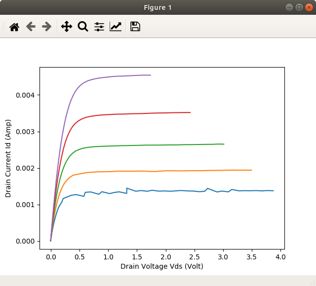
- Below ≈ 1.65 V gate bias, drain current was too small for clear curves in this setup.
- Higher $V_{GS}$ produced larger $I_D$ for the same $V_{DS}$.
- Curves show the expected rise of $I_D$ with $V_{DS}$ then a flatter region at higher $V_{DS}$ (device- and resistor-limited).
8. Precautions
- Keep $R_D = 1\text{ k}\Omega$ in series with the drain — never short PV1 to drain.
- Observe 2N7000 pinout (D / G / S).
- Limit PV1/PV2 to safe SEELab ranges; zero outputs when finished.
- Static-sensitive device — handle with care.
9. Troubleshooting
| Symptom | Possible Cause | Corrective Action |
|---|---|---|
| $I_D \approx 0$ for all PV1 | $V_{GS}$ too low / gate open | Raise PV2 above ~1.65 V; check gate wire |
| $V_{DS} \approx$ PV1 always | MOSFET off or S not grounded | Check source–GND and pinout |
| Excessive current | Missing $R_D$ | Insert 1 kΩ immediately |
10. Viva-Voce Questions
Q1. How is $I_D$ measured without an ammeter?
Ans: From the drop on $R_D$: $I_D = (V_{\text{PV1}} - V_{\text{A1}})/R_D$ with A1 at the drain.
Q2. Why start $V_{GS}$ near 1.65 V for the 2N7000 in this lab?
Ans: Below that gate voltage the device barely conducts in this resistor-limited setup, so $I_D$–$V_{DS}$ curves are not useful.
Q3. What is the role of PV1 vs PV2?
Ans: PV2 sets gate–source bias ($V_{GS}$); PV1 sweeps the drain supply so $V_{DS}$ and $I_D$ can be traced for each gate setting.