

Logic Gates using TTL ICs and Diodes
Adapted from the ExpEYES blog lab on digital AND/OR gates. Study 74LS08 (AND) and 74LS32 (OR), then rebuild the same functions with diodes.
1. Aim
To verify the truth tables of AND and OR gates using TTL ICs driven by SEELab square waves, and to implement the same logic with discrete diodes.
2. Apparatus / Components Required
- SEELab3 / ExpEYES-17 (SQ1, SQ2 / WG-as-SQ2, A1, A2, A3, +5 V or OD1)
- 74LS08 quad 2-input AND
- 74LS32 quad 2-input OR (pin-compatible package)
- Diodes (e.g. 1N4148), resistors for diode logic and A3 protection
- Breadboard and wires
3. Theory & Principle
| Gate | Output HIGH when |
|---|---|
| AND | Both inputs HIGH |
| OR | At least one input HIGH |
TTL inputs are driven by SQ1 and SQ2. Measure inputs on A1/A2 (16 V range) and output on A3 through a series resistor (A3 range is only $\pm 3.3\text{ V}$).
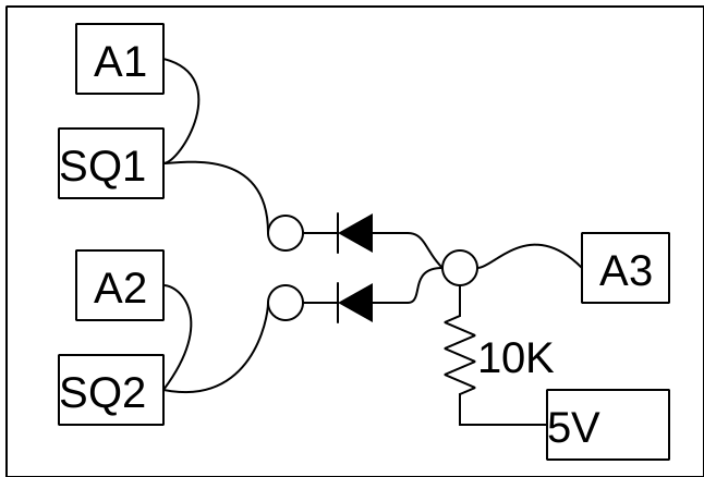
Diode AND: If either input goes LOW, a diode conducts and pulls the junction LOW.
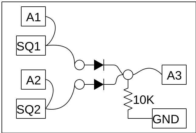
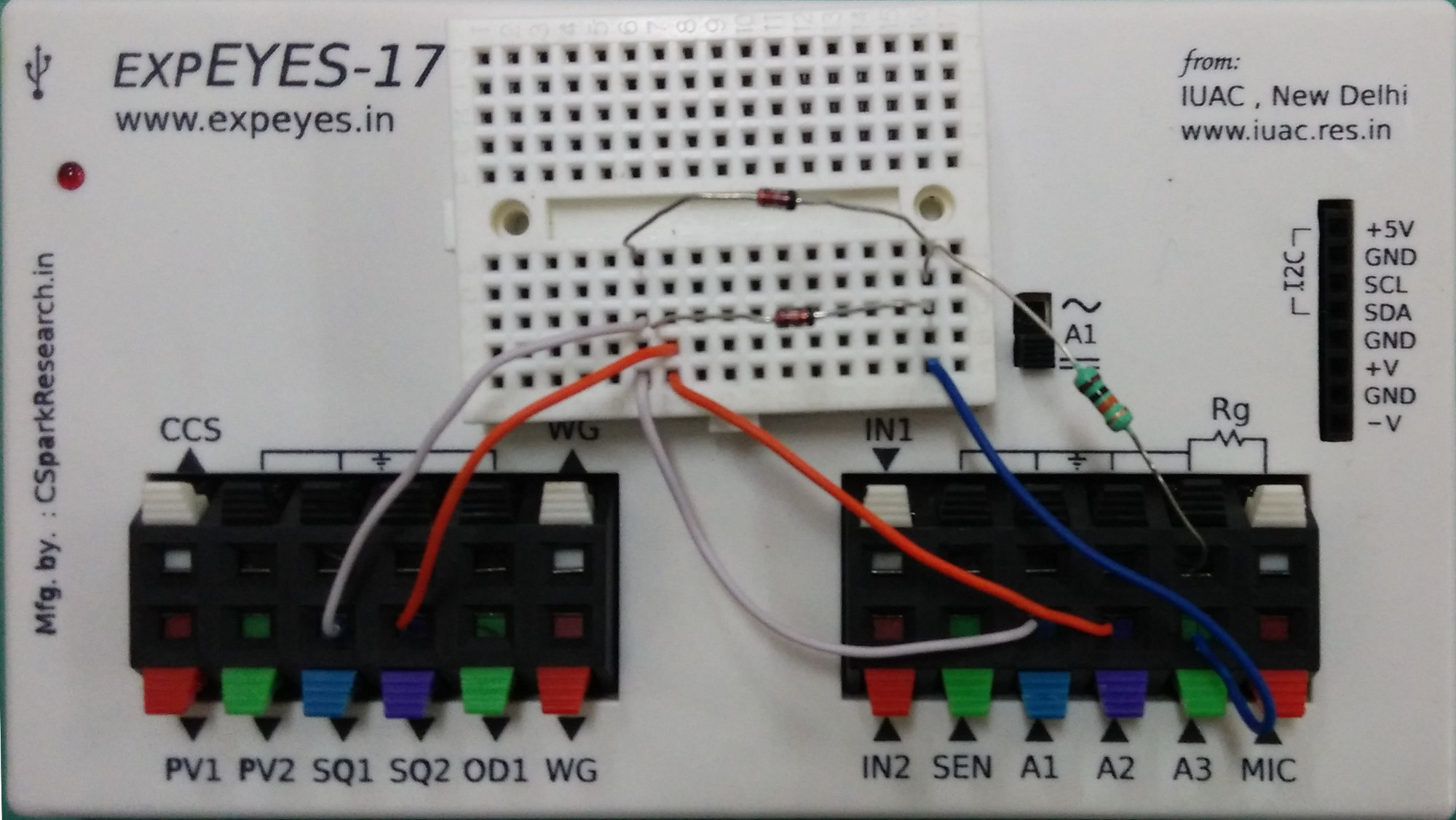
Diode OR: If either input is HIGH, a diode conducts and the output goes HIGH.
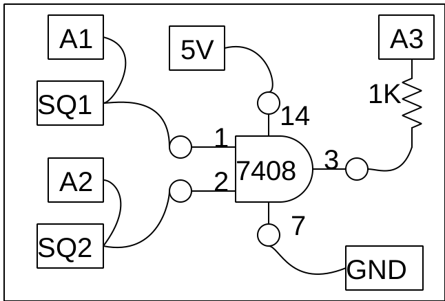
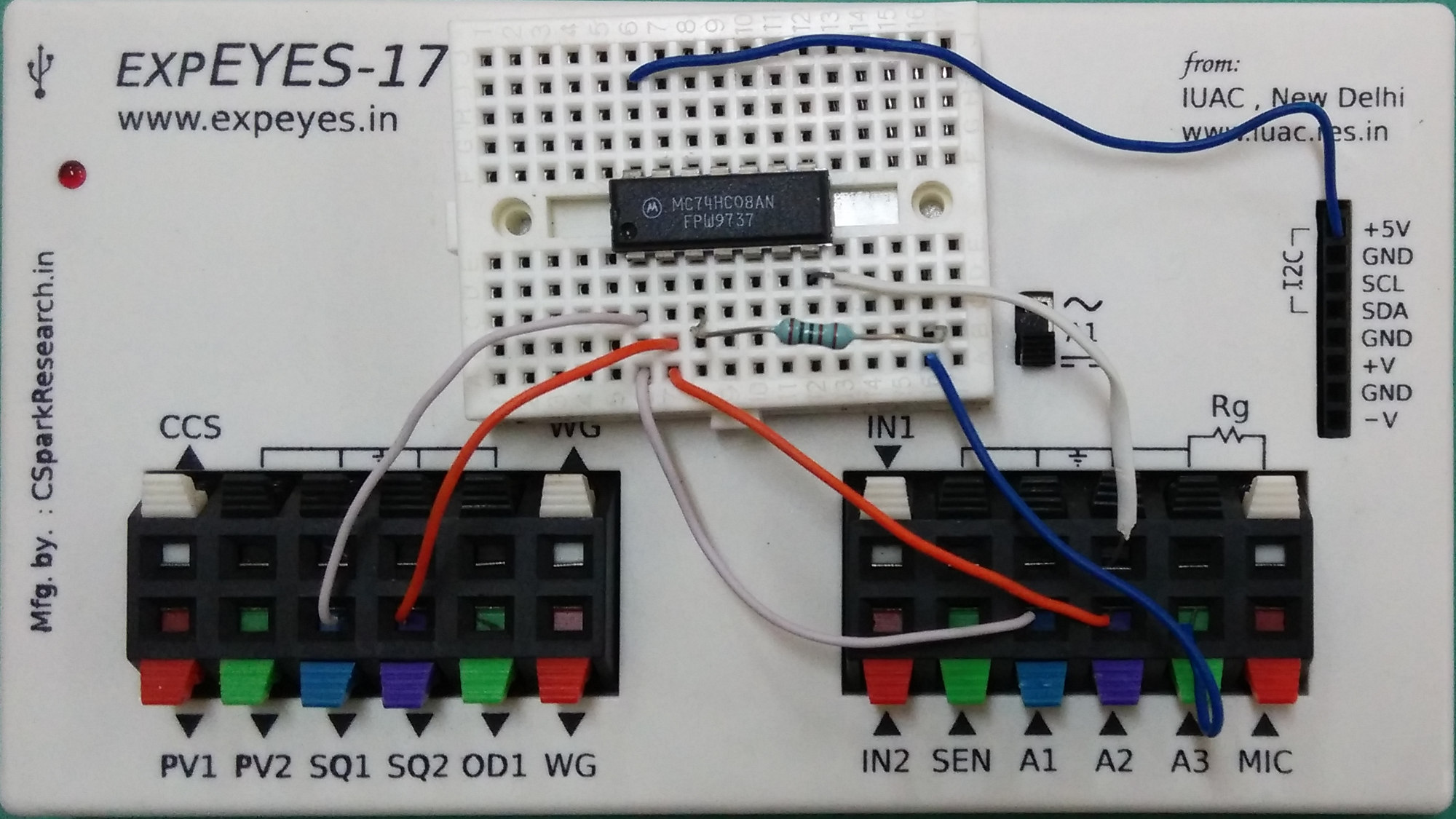
4. Circuit Diagram / Setup — IC AND (74LS08)
- Power the IC from +5 V (or turn OD1 ON and use it as +5 V).
- Connect inputs to SQ1 and SQ2 (set WG to the SQ2 option if required by your UI).
- Connect IC output to A3 via a series resistor.
- Monitor SQ1/SQ2 (or A1/A2) and A3 on the scope; level-shift A1/A2 if traces overlap.
5. Procedure
Part A — AND (74LS08)
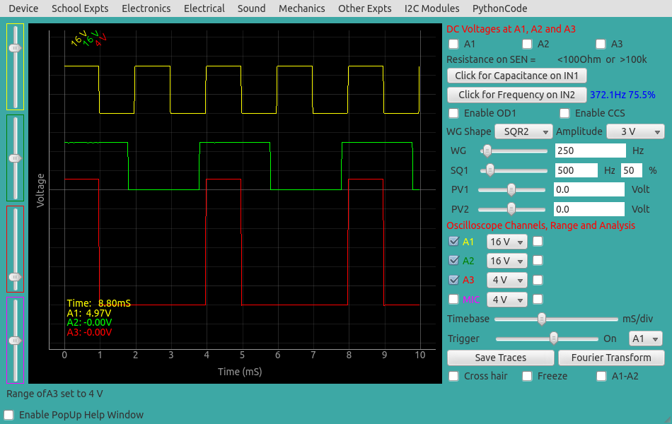
- Build the AND circuit and enable SQ1/SQ2.
- Observe that the red output (A3) is HIGH only when both inputs are HIGH.
- Fill the truth table from the waveforms.
Part B — OR (74LS32)
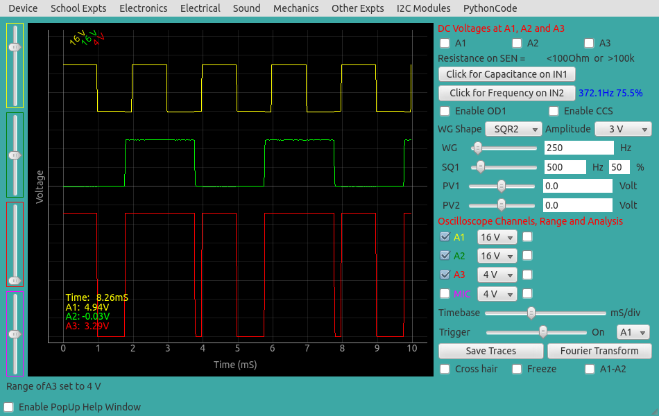
- Replace 74LS08 with 74LS32 (same pinout for a single gate in this wiring).
- Confirm the output is HIGH when either input is HIGH.
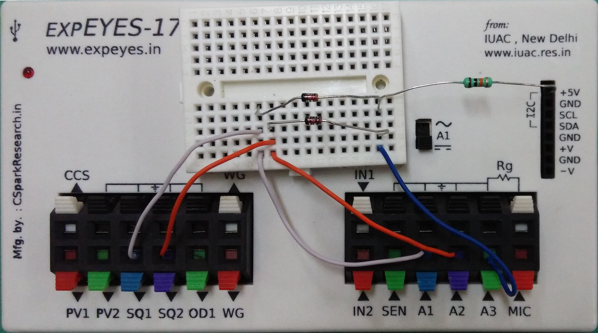
Part C — Diode AND
- Build the diode AND network as in the schematic; drive with SQ1/SQ2; observe output.
Part D — Diode OR
- Build the diode OR circuit and compare with the 74LS32 waveforms.
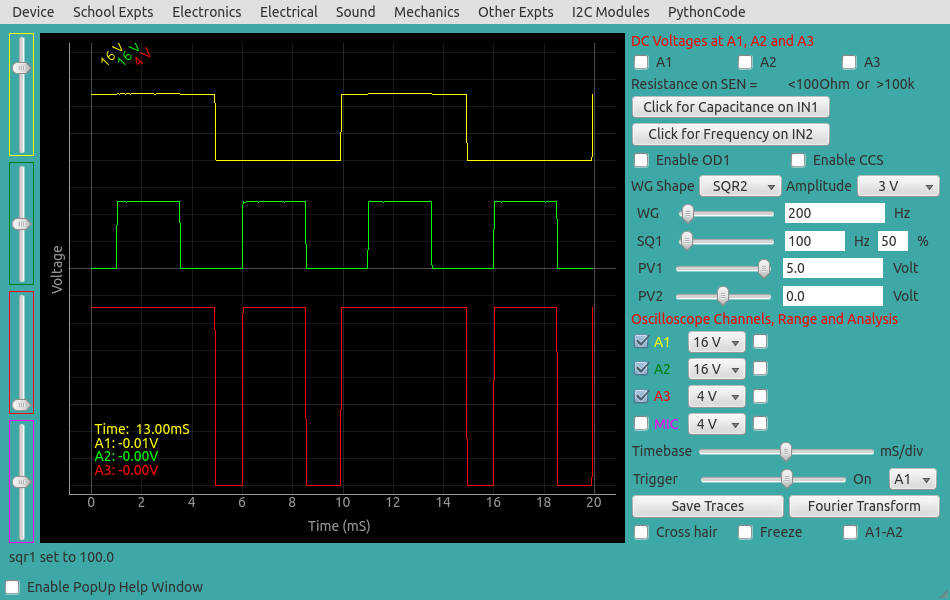
6. Observation Table
6a. AND (74LS08)
| SQ1 | SQ2 | Output (A3) | Matches AND? |
|---|---|---|---|
| L | L | ||
| L | H | ||
| H | L | ||
| H | H |
6b. OR (74LS32) and diode gates
| Gate | Matches TTL OR/AND? | Remarks |
|---|---|---|
| 74LS32 OR | ||
| Diode AND | ||
| Diode OR |
7. Results and Discussion
- TTL AND output was HIGH only for both inputs HIGH.
- TTL OR matched the OR truth table after swapping to 74LS32.
- Diode logic reproduced the same Boolean functions with different voltage levels / noise margins.
8. Precautions
- Always use a series resistor into A3 (3.3 V range).
- Do not exceed TTL input ratings; use SEELab SQ levels appropriately.
- OD1 must be ON if used as +5 V.
- Observe ESD care with CMOS/TTL ICs.
9. Troubleshooting
| Symptom | Possible Cause | Corrective Action |
|---|---|---|
| Flat output | IC unpowered | Check +5 V / OD1 |
| A3 clipped / wrong | No series resistor | Add series R into A3 |
| Overlapping traces | Same DC offset | Level-shift A1/A2 in software |
10. Viva-Voce Questions
Q1. Why monitor the IC output on A3 rather than A1?
Ans: A3 has a smaller range suited to 0–5 V logic after attenuation; A1/A2 are reserved for viewing the higher-swing square inputs with flexible ranging.
Q2. How does a diode AND implement the AND function?
Ans: A LOW on either input forward-biases a diode and pulls the output node LOW. The output stays HIGH only if both diodes are off (both inputs HIGH).
Q3. Why are 74LS08 and 74LS32 convenient as a pair in this lab?
Ans: They are pin-compatible for the gate used here, so OR can be measured by swapping the IC without rewiring the board.