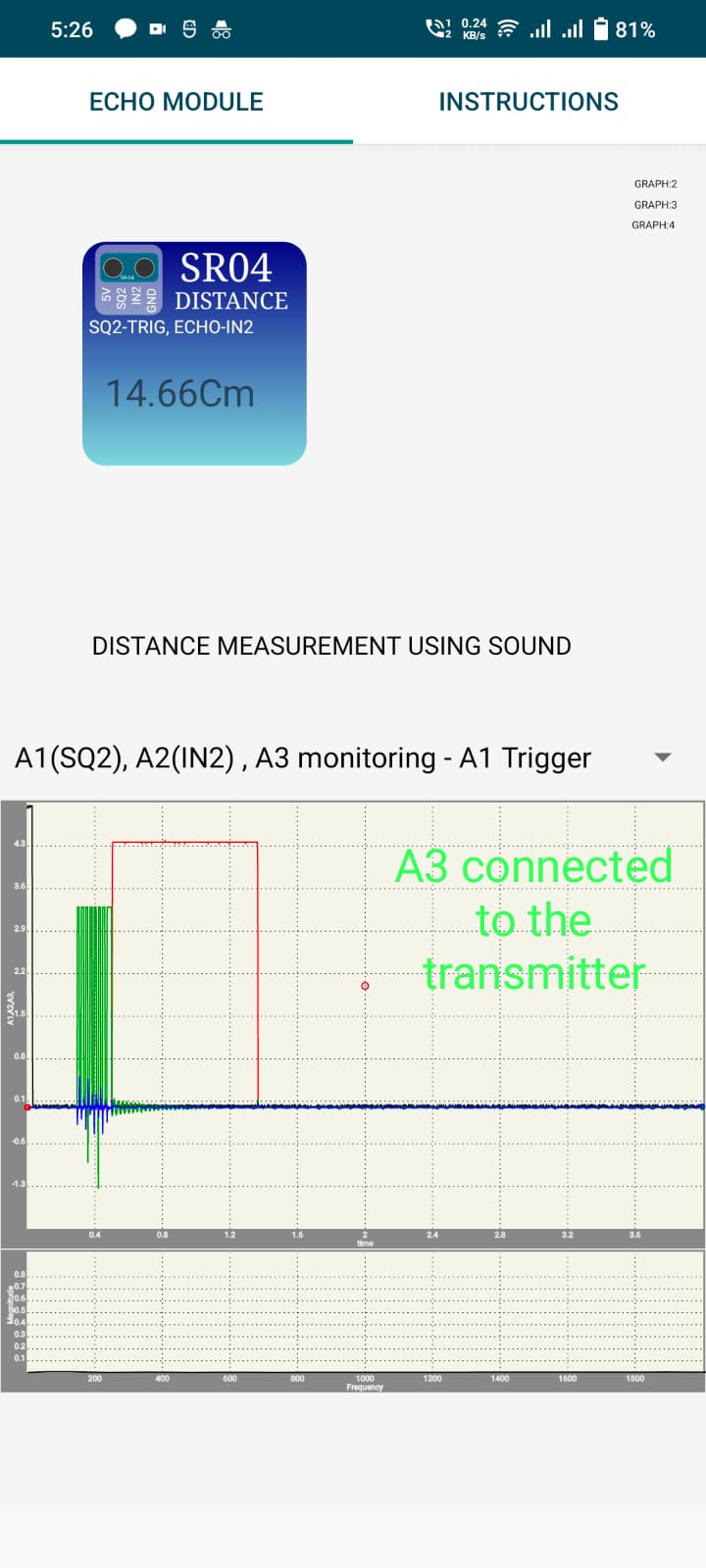
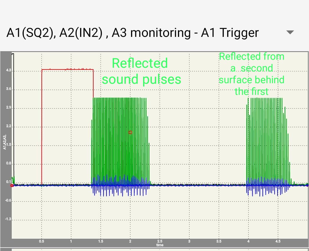
-Distance Measurement using SR04 Ultrasonic Module
Chapter 6: Acoustics
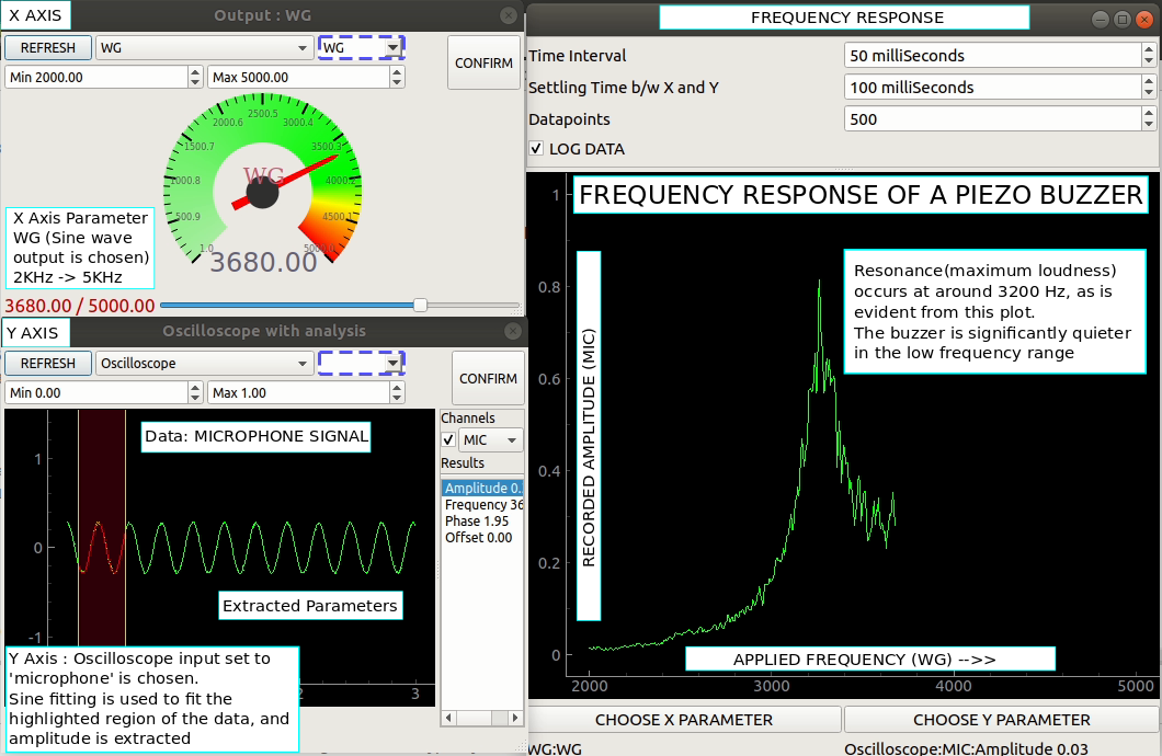
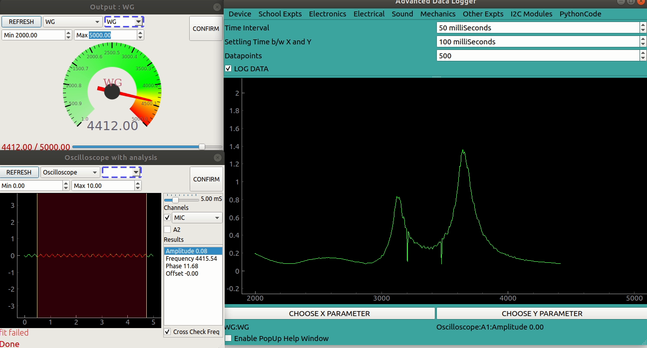
-Frequency Response of Piezo Buzzer
-Interference of Sound (Beats)
-Velocity of Sound in Air
Chapter 7: Interfacing
-Diode I–V Characteristics (Python / eyes17)
-NPN Common-Emitter Output (Python / eyes17)
Chapter 8: advanced
-Sensor Oscilloscope for accelerometers and gyroscopes
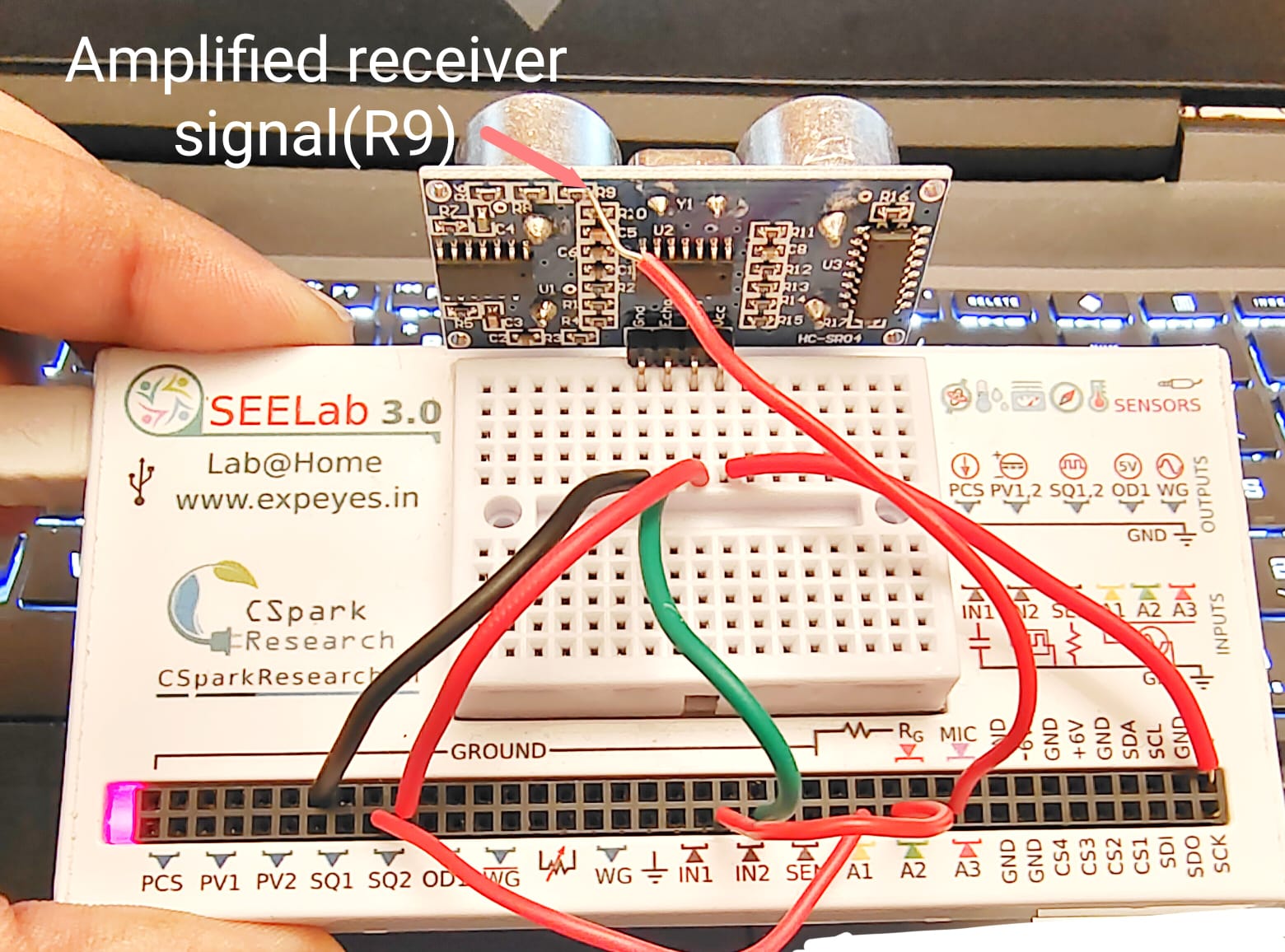
-Pulling apart the SR04 Echo based Distance sensor
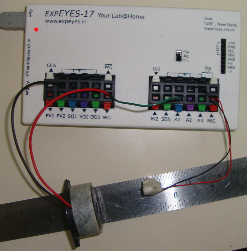
-Piezo buzzer resonance with a square wave generator
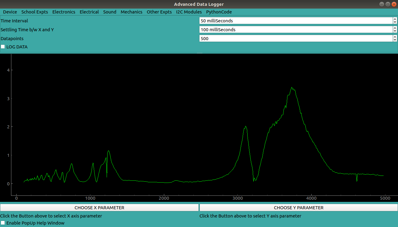
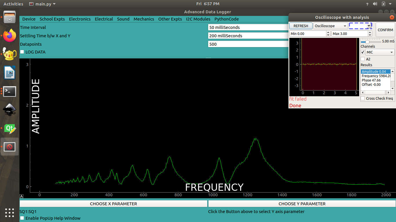
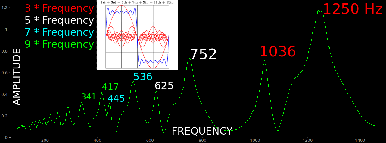
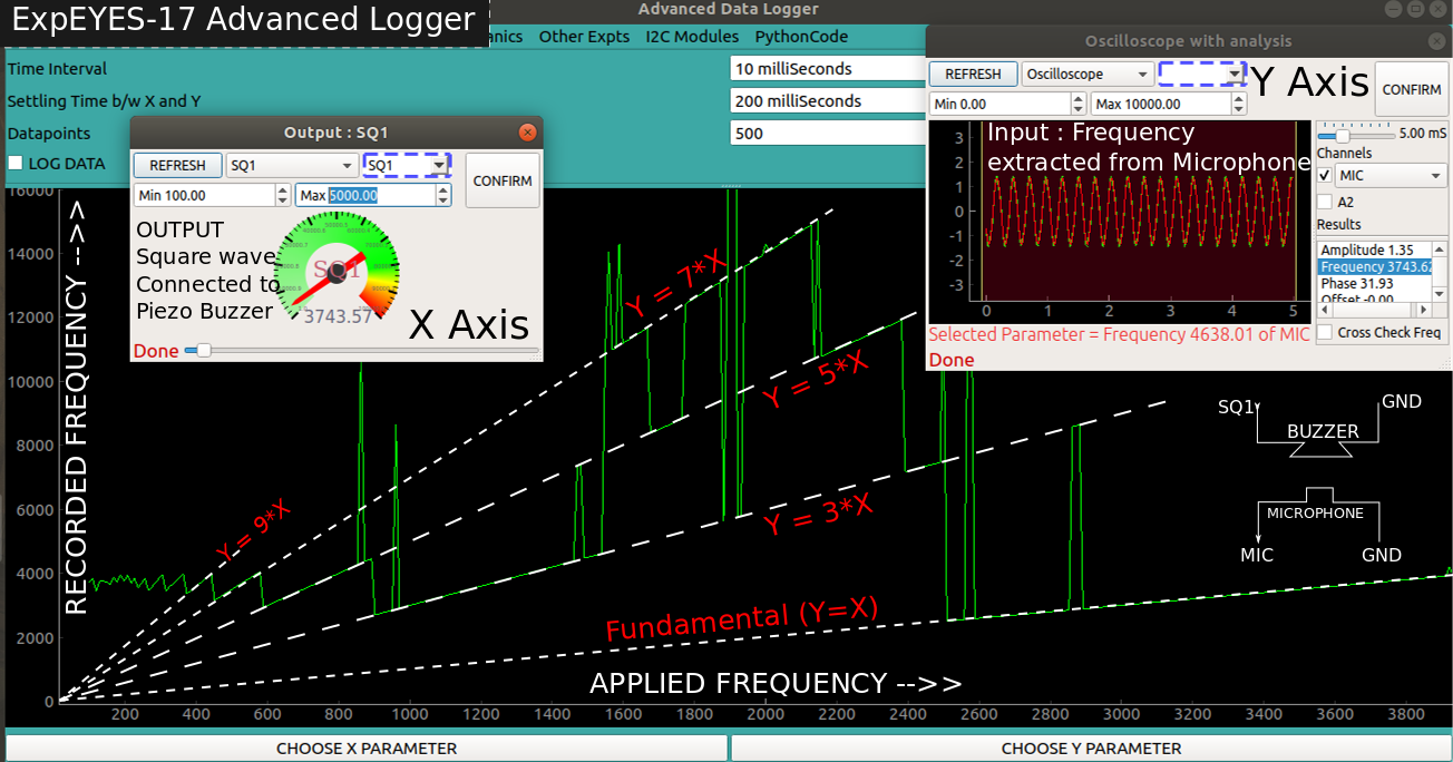
-Advanced Data Logger
Section
Chapter 1: Getting Started
Chapter 1: Getting Started
Measuring DC Voltage on a Single Input
Experiment
Measuring DC Voltage on a Single Input
Measurement of DC Voltage on One Analog Input
1. Aim
To measure a DC voltage using one selected analog input of SEELab3/ExpEYES (A1, A2, or A3) with respect to GND.
2. Apparatus / Components Required
SEELab3 or ExpEYES-17 unit
Connecting wires
A DC source (single cell, battery pack, PV1/PV2, or lab supply)
A PC, Laptop, or Android Phone with SEELab3 software
3. Theory & Principle
The analog inputs of SEELab3 act as digital voltmeters (12 bit resolution).
Use only one input at a time for now:
A1 or A2: wider range, typically about $\pm16V$, but can also measure smaller signals down to $\pm250mV$ using the built-in amplifier.
A3: higher input impedance and better low-voltage use. Fixed range of $\pm3.3V$
Always measure voltage with respect to GND:
\(V_{\text{measured}} = V(\text{Input}) - V(\text{GND})\)
4. Circuit Diagram / Setup
Select one channel: A1 (or A2 or A3).
Connect source negative to GND.
Connect source positive to the selected input.
Open the voltage-measurement tool in software.
5. Procedure
Start with a small DC source (for example, a 1.5V cell).
Note the reading on the selected input.
Reverse leads once to observe sign change (+V becomes -V).
For batteries in series:
Measure one cell.
Then measure two cells in series.
Then measure three cells in series (if expected value is within channel limit).
In the mobile app, you can select the voltage range by clicking on the range button at the top right corner of the graph.
Record all readings and compare with expected sums.
6. Observation Table
Selected Input
Source
Expected Voltage (V)
Measured Voltage (V)
Remarks
Single cell (1.5V)
Two cells in series
Three cells in series
7. Error Analysis
Possible causes of small mismatch:
Source internal resistance: meter loading can reduce measured voltage if it’s a very weak source.
Input impedance effect: A1/A2 (about $1M\Omega$) load more than A3 (about $10M\Omega$).
ADC resolution and offset: small quantization and zero-offset errors are normal.
8. Results and Discussion
DC voltage was measured correctly on one selected input.
Series battery voltages approximately added:
\(V_{\text{series}} \approx V_1 + V_2 (+V_3)\)
A3 generally shows less loading error for high-resistance sources.
9. Precautions
Voltage limits are critical:
A1, A2: keep within about $\pm16V$
A3: keep within about $\pm3.3V$
Battery checks:
1 cell (AA): ~1.2 to 1.6V
2 cells in series: ~2.4 to 3.2V (safe on A3, near upper side for fresh cells)
3 cells in series: ~3.6 to 4.8V (do not use A3, use A1/A2)
Use common GND.
Do not leave input floating during observation .
10. Troubleshooting
Symptom
Possible Cause
Corrective Action
Reading stays near 0V
Wrong/loose connection
Recheck GND and selected input wiring
Reading clipped at limit
Input over-range
Shift from A3 to A1/A2, reduce source voltage
Reading lower than expected
Loading by input impedance
Use A3 for high-resistance sources
Noisy trace
Floating input
Connect input properly to source or GND
Device not found
Connection issue.
Reconnect the USB cable and restart the software.
11. Viva-Voce Questions
Q1. Why do we connect source negative to GND?
Ans: Voltage is measured relative to a reference. `GND` is that 0V reference for SEELab.
Q2. Which input is safer for 3 cells in series (~4.5V)?
Ans: `A1` or `A2`. `A3` should be kept within about $\pm3.3V`.
Q3. Why can readings differ between A1 and A3 for high-resistance sources?
Ans: Input impedance differs. A lower impedance meter loads the circuit more and can pull the measured node voltage down.
Q4. If a 3V source is connected to A1 through a 1MΩ series resistor, what will be displayed?
Ans: Model it as a divider: source -- $1M\Omega$ -- input impedance to ground.
For A1, $R_{\text{in}} \approx 1M\Omega$:
$$
V_{A1}=3\times\frac{1}{1+1}=1.5V
$$
So the displayed voltage is approximately 1.5V.
Q5. For the same setup (3V through 1MΩ), what will A3 show if A3 input impedance is 10MΩ?
Ans: Again divider rule:
$$
V_{A3}=3\times\frac{10}{1+10}=3\times\frac{10}{11}\approx2.73V
$$
So A3 shows approximately 2.73V, closer to the true source voltage because of higher input impedance.
Chapter 1: Getting Started
Measuring Resistance using SEN
Experiment
Measuring Resistance using SEN
Measuring Resistance
1. Aim
To measure an unknown resistance connected between SEN and GND using SEELab/ExpEYES.
2. Apparatus / Components Required
SEELab3 or ExpEYES-17 unit
Resistors (typical range: 100 ohm to 100 kohm)
Connecting wires
PC/Laptop/Android phone with SEELab software
3. Theory & Principle
Inside ExpEYES, SEN is connected to 3.3V through an internal 5.1 kohm resistor.
When an unknown resistor R is connected from SEN to GND, a voltage divider is formed.
\[V_{SEN}=3.3\cdot\frac{R}{R+5100}\]
Hence,
\(R=5100\cdot\frac{V_{SEN}}{3.3-V_{SEN}}\)
Best accuracy is obtained when R is of the same order as 5.1 kohm.
4. Circuit Diagram / Setup
Connect one terminal of unknown resistor to SEN.
Connect other terminal to GND.
Open “Measure Resistance” in software/app.
5. Procedure
Start with a known resistor (for example 1 kohm) for verification.
Note displayed resistance.
Repeat for 470 ohm, 2.2 kohm, 10 kohm, 47 kohm.
Compare measured and nominal values.
For unknown resistor, repeat measurement 3 times and average.
6. Observation Table
Nominal Resistance
Measured Resistance
% Error
Remarks
470 ohm
1 kohm
2.2 kohm
10 kohm
47 kohm
7. Series and Parallel Combinations
Use two known resistors (example: R1 = 1 kohm, R2 = 2.2 kohm) and verify equivalent resistance.
For series:
\(R_{series}=R_1+R_2\)
For parallel:
\(R_{parallel}=\frac{R_1R_2}{R_1+R_2}\)
Procedure:
Measure R1 and R2 individually.
Connect R1 and R2 in series between SEN and GND, then measure.
Connect R1 and R2 in parallel between SEN and GND, then measure.
Compare measured equivalents with calculated values.
Combination
Calculated Equivalent
Measured Equivalent
% Error
R1 alone
R2 alone
R1 + R2 (series)
R1 || R2 (parallel)
8. Advanced: Manual Calculation from SEN Voltage
If software shows V_SEN, calculate R manually using:
\(R=5100\cdot\frac{V_{SEN}}{3.3-V_{SEN}}\)
Example: if V_SEN = 1.65V,
\(R=5100\cdot\frac{1.65}{1.65}=5100\ \Omega\)
9. Error Analysis
Measurement is less accurate at very low (<<100 ohm) or very high (>>100 kohm) resistance.
Internal resistor tolerance and ADC resolution introduce small errors.
10. Precautions
Keep resistor leads firm and clean.
Do not apply external voltage directly to SEN in this experiment.
Use dry fingers / insulated clips; finger touch may alter high values.
11. Troubleshooting
Symptom
Possible Cause
Corrective Action
Reads nearly 0 ohm
Short circuit in wiring
Recheck connections
Reads very high / overflow
Open circuit / loose lead
Tighten clips
Reading unstable
Poor contact
Clean terminals and reconnect
12. Viva-Voce Questions
Q1. Why is resistance measured between SEN and GND?
Ans: Because SEN has a known internal resistor to 3.3V, making a divider with the unknown resistor to GND.
Q2. Why is measurement most accurate near a few kohms?
Ans: Maximum sensitivity occurs when unknown resistance is comparable to the internal 5.1 kohm resistor.
Q3. What is the approximate measurable range?
Ans: Roughly 100 ohm to 100 kohm for useful accuracy.
Chapter 1: Getting Started
Measuring Capacitance using IN1
Experiment
Measuring Capacitance using IN1
Measuring Capacitance
1. Aim
To measure capacitance connected between IN1 and GND, and study how geometry affects capacitance.
2. Apparatus / Components Required
SEELab3 or ExpEYES-17 unit
Capacitors of known values
Connecting wires / crocodile clips
Two foil plates + paper/plastic sheet (for homemade capacitor)
PC/Laptop/Android phone with SEELab software
3. Theory & Principle
Capacitance is defined as:
\(C=\frac{Q}{V}\)
SEElab measures small capacitances (pF and nF ranges) by charging with a constant current source and measuring the voltage rise produced. Q is the product of C and V, and Q can be calculated as a product of this constant current and the time spent charging.
For a parallel-plate capacitor:
\(C\propto\frac{A}{d}\)
More explicitly (same dielectric):
\(C = \epsilon \frac{A}{d}\)
where A is plate overlap area and d is separation.
For larger values, it charges the capacitor via a built-in 10K resistor whilst simultaneously capturing the capacitor voltage using the oscilloscope. All this magic happens internally, and the capacitance value is extracted after fitting the charging curve to an appropriate function to extract the time constant.
Mobile App
Photo with ExpEYES17
4. Circuit Diagram / Setup
Connect capacitor between IN1 and GND.
Open the “Measure Capacitance” tool and trigger measurement.
Repeat with different capacitors.
5. Procedure
Measure known capacitors and record values.
Build a parallel-plate capacitor using foil-paper-foil.
Measure capacitance for full overlap.
Reduce overlap area gradually and re-measure.
Compare trends in measured values.
6. Observation Table
Capacitor Type
Expected Value
Measured Value
Remarks
Ceramic (nominal)
Electrolytic (nominal)
Homemade plate capacitor (full area)
Homemade plate capacitor (reduced area)
7. Advanced: Area Dependence Check
For same dielectric and separation:
\(\frac{C_2}{C_1} \approx \frac{A_2}{A_1}\)
Example: if overlap area is reduced to half, measured capacitance should be approximately half.
8. Error Analysis
Stray capacitance of wires and surroundings affects small-capacitance readings.
Touching plates with fingers adds parallel leakage paths and body capacitance.
Poor clip contacts and unstable setup can cause fluctuations.
9. Precautions
Do not touch capacitor plates during measurement.
Keep leads short for pF-range measurements.
Ensure capacitor is discharged before reconnecting.
Q1. Why should you not touch capacitor plates while measuring?
Ans: Touch introduces leakage and extra capacitance, changing measured value.
Q2. How does capacitance change with plate overlap area?
Ans: Capacitance is directly proportional to overlap area.
Q3. What happens when plate separation increases?
Ans: Capacitance decreases because $C$ is inversely proportional to separation.
Chapter 1: Getting Started
Measuring Multiple DC Voltages
Experiment
Measuring Multiple DC Voltages
Measurement of DC Voltages on A1, A2, and A3
1. Aim
To measure and display DC voltages applied to the analog input terminals (A1, A2, and A3) of the SEELab3/ExpEYES device and to observe voltage variations over time.
2. Apparatus / Components Required
SEELab3 or ExpEYES-17 unit
Connecting wires
A regulated DC power source (e.g., PV1, PV2, or a battery/cell)
A PC, Laptop, or Android Phone with SEELab3 software
3. Theory & Principle
The analog inputs A1, A2, and A3 on the SEELab3 function as digital voltmeters.
A1 and A2: Designed for general purpose use with a wider input range (typically $\pm 16V$).
A3: Optimized for high sensitivity with a smaller range (typically $\pm 3.3V$).
The device utilizes an Analog-to-Digital Converter (ADC) to translate continuous voltage levels into digital values. In “Multimeter” mode, the software displays instantaneous values. In “Oscilloscope” or “Plot” mode, it tracks these values over time ($t$), allowing you to visualize the stability of a DC source.
4. Circuit Diagram / Setup
Connect the Ground (GND) terminal of the SEELab3 to the negative terminal of the voltage source.
Connect the positive terminal of the voltage source to the A1, A2, or A3 input.
Self-Test: You can connect PV1 to A1 to measure the voltage generated by the SEELab3 device itself.
5. Procedure
Open the SEELab3 software and select the “Measure Voltages” or “Multimeter” experiment.
Instantaneous View: Observe the live digital display for each channel. If using PV1 as a source, adjust the slider and watch the reading on A1 change accordingly.
Time-Domain View: Switch to the “Plot” or “Oscilloscope” mode.
Observe the horizontal trace. A steady DC voltage should appear as a perfectly flat line.
Sensitivity Check: Connect a small 1.5V cell to A3 and then to A1 to compare the precision of the readings.
6. Observation Table
Input Channel
Source Type (e.g., Battery, PV1)
Measured Voltage (V)
Remarks (Stability)
A1
A2
A3
7. Error Analysis
While digital voltmeters are highly accurate, small discrepancies can occur due to:
Resolution Limits: The ADC has a finite number of bits. On a $16V$ range, a 12-bit ADC has a resolution of roughly $16/4096 \approx 4\text{ mV}$. Changes smaller than this cannot be detected.
Input Impedance: A1 and A2 typically have an input impedance of $1\text{ M}\Omega$. If measuring a source with very high internal resistance, the voltmeter itself might “load” the circuit, causing a lower voltage reading.
Zero Offset: Even with no input, the software might show a few millivolts (e.g., $0.003V$). This is a common calibration offset.
8. Results and Discussion
The DC voltages applied to inputs A1, A2, and A3 were measured accurately.
The software plotting feature allowed for the observation of voltage stability over the measured time interval.
It was observed that A3 provides higher precision for low-voltage signals compared to A1.
9. Precautions
Voltage Limits: Do not exceed $\pm 16V$ on A1/A2. Exceeding $\pm 3.3V$ on A3 may clip the signal or trigger protection circuits.
Common Ground: The measurement is always relative to GND. Ensure the ground is common between the source and the SEELab.
Input Floating: If nothing is connected to an input, it may “float” and show random, rapidly changing values due to electromagnetic interference.
10. Troubleshooting
Symptom
Possible Cause
Corrective Action
Reading stays at 0V
Loose connection.
Check both the GND and the Input terminal wires.
Reading is ‘Maxed Out’
Voltage exceeds range.
Move the connection to a channel with a higher range (e.g., A3 to A1).
Noisy Graph Trace
Floating input.
Connect the input to a known source or GND to see if the noise stops.
Device not found
Connection issue.
Reconnect the USB cable and restart the software.
11. Viva-Voce Questions
Q1. What is the function of an ADC in SEELab3?
Ans: The Analog-to-Digital Converter (ADC) converts continuous analog voltage signals into discrete digital numbers that the computer or smartphone software can process and display.
Q2. Why is it important to connect the GND terminal?
Ans: Voltage is a measure of potential difference. The GND terminal acts as the 0V reference point. Without a common ground, the device cannot accurately determine the potential level of the input signal.
Q3. Which channel (A1 or A3) should you use to measure a 1.2V AA battery? Why?
Ans: A3 is better because it has a smaller input range ($\pm 3.3V$) and therefore offers higher resolution and sensitivity for low-voltage signals.
Q4. What does a "steady DC voltage" look like on an oscilloscope/plot?
Ans: It appears as a flat, horizontal straight line, indicating that the voltage value is constant over time.
Q5. What happens if you connect a voltage higher than 16V to A1?
Ans: The reading will "saturate" or "clip" at the maximum limit (e.g., 16.5V). While the device has protection diodes, repeatedly exceeding these limits can damage the input circuitry.
Chapter 1: Getting Started
Study of Light Dependent Resistor (LDR)
Experiment
Study of Light Dependent Resistor (LDR)
Study of Light Dependent Resistor (LDR)
1. Aim
To study variation of LDR resistance with light intensity using SEN and GND.
2. Apparatus / Components Required
SEELab3 or ExpEYES-17 unit
LDR
Connecting wires
Light source (phone torch / LED lamp)
PC/Laptop/Android phone with SEELab software
3. Theory & Principle
LDR resistance decreases when light intensity increases.
In this experiment, LDR is connected between SEN and GND. Internally, SEN is connected to 3.3V through 5.1 kohm.
From measured V_SEN, LDR resistance is:
\(R_{LDR}=5100\cdot\frac{V_{SEN}}{3.3-V_{SEN}}\)
If multiple points are taken, a log plot (\log R vs \log L) can be used to estimate empirical exponent:
\(R\propto L^{-k}\)
8. Error Analysis
Ambient light fluctuations cause drift.
Sensor heating or light-source flicker changes reading.
Shadows and angle of incidence affect effective illumination.
9. Precautions
Keep light source distance fixed for repeated trials.
Avoid hand shadow while recording.
Wait 1-2 seconds after changing light before reading.
Do not apply external voltage directly to SEN.
10. Troubleshooting
Symptom
Possible Cause
Corrective Action
No variation in reading
Wrong wiring / faulty LDR
Recheck LDR between SEN and GND
Reading very noisy
Flickering light source
Use steady DC light source
Saturated high/low value
Too dark / too bright constantly
Adjust illumination range
11. Viva-Voce Questions
Q1. What happens to LDR resistance when light increases?
Ans: LDR resistance decreases as light intensity increases.
Q2. Why is SEN used in this experiment?
Ans: SEN has a known internal resistor to 3.3V, allowing resistance estimation from measured voltage.
Q3. Why can two readings differ even at same lamp brightness?
Ans: Distance/angle changes, ambient light, and LDR response time can alter readings.
Chapter 1: Getting Started
Lemon Cell: Measuring EMF of Metal Pairs
Experiment
Lemon Cell: Measuring EMF of Metal Pairs
Lemon Cell Experiment
1. Aim
To construct a lemon cell and measure the EMF produced by different metal electrode pairs using one SEELab input channel.
2. Apparatus / Components Required
SEELab3 or ExpEYES-17 unit
Connecting wires / crocodile clips
1-2 lemons (or any acidic fruit)
Common metal electrodes (for example: Zinc nail, Copper strip/coin, Iron nail, Aluminium strip)
A PC, Laptop, or Android Phone with SEELab3 software
3. Theory & Principle
A lemon acts as an electrolyte. Two dissimilar metals inserted into the lemon form a galvanic cell.
The open-circuit voltage (EMF) depends on the electrode pair and electrolyte condition.
For this experiment, use one channel (A1 or A3) and measure with respect to GND.
Expected EMF trend follows metal reactivity difference:
larger reactivity difference -> higher EMF
copper is commonly used as the positive electrode in these pairs
Always measure voltage with respect to GND:
\(V_{\text{measured}} = V(\text{Input}) - V(\text{GND})\)
4. Circuit Diagram / Setup
Select one input channel (A1 recommended; A3 is also fine here).
Insert two different metal electrodes into the lemon, separated by ~2-3 cm.
Connect the electrode expected to be negative (e.g., zinc) to GND.
Connect the other electrode (e.g., copper) to the selected input.
Open DC voltage measurement in the SEELab software/app.
5. Procedure
Start with the Zn-Cu pair and note the voltage.
Swap leads once and confirm sign reversal.
Repeat with other pairs (Fe-Cu, Al-Cu, Zn-Fe, etc.).
For each pair, wait 5-10 seconds for reading to stabilize and record value.
Optional: connect two lemon cells in series and verify voltage addition.
Mobile App
Desktop App
6. Observation Table
Metal Pair
Typical EMF Range in Lemon (V)
Measured Voltage (V)
Remarks
Zn-Cu
0.8 to 1.1
Al-Cu
0.6 to 1.0
Fe-Cu
0.4 to 0.8
Zn-Fe
0.2 to 0.5
Al-Fe
0.1 to 0.4
7. Reference EMF Values (Common Metals)
Approximate standard electrode potentials (vs SHE, at 25 C):
Metal / Electrode
$E^\circ$ (V)
Zn / Zn$^{2+}$
-0.76
Al / Al$^{3+}$
-1.66
Fe / Fe$^{2+}$
-0.44
Cu / Cu$^{2+}$
+0.34
Approximate ideal EMF for common pairs (difference of $E^\circ$):
Pair (Anode-Cathode)
Ideal $\Delta E^\circ$ (V)
Al-Cu
2.00
Zn-Cu
1.10
Fe-Cu
0.78
Al-Fe
1.22
Zn-Fe
0.32
In real lemon cells, measured values are usually lower due to internal resistance, polarization, oxide layers, and non-standard ion concentrations.
8. Advanced: Estimating Internal Resistance of Lemon Cell
Model the lemon cell as an ideal source $E$ in series with internal resistance $r$.
When connected to a voltmeter of input resistance $R_{in}$, measured terminal voltage is:
\(V = E\cdot\frac{R_{in}}{r+R_{in}}\)
For this experiment:
A1 input resistance $R_{A1}\approx1M\Omega$
A3 input resistance $R_{A3}\approx10M\Omega$
Steps
Build one lemon cell (for example Zn-Cu).
Measure open terminal voltage with A1: call it $V_{A1}$.
Measure same cell with A3: call it $V_{A3}$.
Use the formula below to estimate $r$.
From two readings:
\(r=\frac{R_{A1}R_{A3}(V_{A3}-V_{A1})}{V_{A1}R_{A3}-V_{A3}R_{A1}}\)
Then estimate EMF:
\(E=V_{A1}\left(1+\frac{r}{R_{A1}}\right)\)
Worked Example
Suppose measured values are:
$V_{A1}=0.60V$
$V_{A3}=0.90V$
Using $R_{A1}=1M\Omega$, $R_{A3}=10M\Omega$:
\(r=\frac{(1)(10)(0.90-0.60)}{(0.60)(10)-(0.90)(1)}M\Omega
=\frac{3}{5.1}M\Omega\approx0.588M\Omega\)
So internal resistance is about:
\(r\approx5.9\times10^5\Omega\)
Now EMF:
\(E\approx0.60\left(1+\frac{0.588}{1}\right)\approx0.95V\)
Ans: Two dissimilar metals in an electrolyte form an electrochemical cell. Their different electrode potentials create an EMF.
Q2. Why is Zn-Cu usually higher than Zn-Fe in a lemon cell?
Ans: The electrode potential difference for Zn-Cu is larger than Zn-Fe, so EMF is generally higher.
Q3. Why are measured lemon-cell voltages lower than ideal EMF values?
Ans: Due to internal resistance, polarization, oxide layers, and non-standard chemical conditions.
Q4. If a 3V source is connected to A1 through a 1MΩ resistor, what is the displayed voltage (A1 input impedance = 1MΩ)?
Ans: Using voltage divider:
$$
V_{A1}=3\times\frac{1}{1+1}=1.5V
$$
Displayed value is approximately 1.5V.
Q5. For the same setup, what is displayed on A3 (input impedance = 10MΩ)?
Ans:
$$
V_{A3}=3\times\frac{10}{1+10}=3\times\frac{10}{11}\approx2.73V
$$
A3 shows approximately 2.73V.
Chapter 1: Getting Started
AC Resistance of the Human Body
Experiment
AC Resistance of the Human Body
Measurement of AC Resistance / Impedance of the Human Body
1. Aim
To estimate the human body’s AC impedance using SEELab3 with an AC source (WG) and the built-in high input impedance at A2.
2. Apparatus / Components Required
SEELab3 or ExpEYES-17 unit
Connecting wires and two metal electrodes (coins/plates/strips)
PC / Laptop / Android with SEELab3 software
3. Theory & Principle
This is a measurement using a voltage divider model:
The human body behaves like an impedance $Z_{body}$.
The SEELab3 input at A2 has a known input impedance $R_{in}$, typically about $1\text{ M}\Omega$.
Let:
$V_{A1}$ = RMS voltage at A1 (across the whole divider)
$V_{A2}$ = RMS voltage at A2 (across $R_{in}$)
Current through the series path is:
\(I=\frac{V_{A2}}{R_{in}}\)
Voltage across the body is:
\(V_{body}=V_{A1}-V_{A2}\)
So the estimated impedance is:
\(Z_{body}=\frac{V_{body}}{I}=(V_{A1}-V_{A2})\cdot\frac{R_{in}}{V_{A2}}\)
For comparison/learning (at moderate frequency like 1000 Hz), $Z_{body}$ can be reported in kilo-ohms.
4. Circuit Diagram / Setup
Connect the AC source WG (sine wave) to one electrode and also to A1 for monitoring.
Connect the other electrode to A2.
Ensure SEELab3 GND reference is correctly wired (as per your hardware).
Keep electrode contact area similar between trials.
5. Procedure
Launch the SEELab3 app and open the AC resistance / impedance measurement screen (or oscilloscope/plot mode with $V_{rms}$ readouts).
Set:
WG frequency = 1000 Hz
WG amplitude = start with a moderate value so RMS voltages stay within A1/A2 range.
Enable analysis/readout for:
A1 (input RMS)
A2 (output RMS)
Touch the electrodes with intact skin and hold contact stable for 3–5 seconds.
Record:
$V_{A1,\text{rms}}$
$V_{A2,\text{rms}}$
Calculate $Z_{body}$ using $R_{in}=1\text{ M}\Omega$:
\(Z_{body}=(V_{A1}-V_{A2})\cdot\frac{10^6}{V_{A2}}\)
Repeat for different contact conditions (dry, wet, increased contact area).
6. Observation Table
Reference: $R_{in} = 1.0\text{ M}\Omega$
Condition
$V_{A1}$ RMS (V)
$V_{A2}$ RMS (V)
Estimated $Z_{body}$ (k$\Omega$)
Remarks
Dry hands
Dry hands with coin/contact increase
Wet hands
7. Precautions
Use only the low voltage AC output from SEELab3 (WG). Never connect to AC mains.
Do not touch with cut/bruised skin or if you have any wound.
Keep contact stable to avoid large fluctuations.
8. Error Analysis
At AC frequencies, the body impedance includes non-resistive components (skin capacitance), so $Z_{body}$ is an approximation.
Contact pressure and contact area change $Z_{body}$ during measurement.
Noise/trigger settings can affect RMS estimation.
9. Troubleshooting
Symptom
Possible Cause
Corrective Action
RMS values look wrong or unstable
Weak/no contact between electrodes and skin
Reposition electrodes; maintain steady touch
$V_{A2}$ is very small
Divider is not formed correctly
Verify WG→electrode→body→A2 path
Computed $Z_{body}$ is unrealistically low/high
Wrong electrode polarity or wiring
Swap electrode connections and retake
10. Viva-Voce Questions
Q1. Why do we need the high input impedance at A2?
Ans: Human body resistance is typically very high (often in the M$\Omega$ / hundreds of k$\Omega$ range). A high $R_{in}$ ensures the divider current is measurable and the voltage drop can be detected.
Q2. Derive the formula for $Z_{body}$ from $V_{A1}$ and $V_{A2}$.
Ans: Current is $I=V_{A2}/R_{in}$. Body voltage is $V_{body}=V_{A1}-V_{A2}$. So $Z_{body}=V_{body}/I=(V_{A1}-V_{A2})\cdot R_{in}/V_{A2}$.
Q3. Why does wetting hands decrease the measured resistance?
Ans: Water (with dissolved salts) improves ionic conduction through skin, reducing resistance/impedance and increasing divider current.
Q4. Is $Z_{body}$ purely resistive at AC?
Ans: No. Skin and electrode interfaces add non-ideal effects (capacitive/complex impedance), but divider-based measurement still gives a useful estimate for comparison.
Chapter 1: Getting Started
DC Resistance of Humans
Experiment
DC Resistance of Humans
Measurement of DC Resistance of the Human Body
1. Aim
To measure the electrical resistance offered by the human body to a DC voltage using the SEELab3/ExpEYES toolkit and to observe how physical conditions like moisture and contact area affect this value.
2. Apparatus / Components Required
SEELab3 or ExpEYES-17 Test & Measurement Tool
Set of connecting wires
A PC, Laptop, or Android Phone with SEELab3 software installed
Metal coins (optional, to test the effect of surface area)
3. Theory & Principle
The human body acts as a conductor, though it offers significant resistance primarily due to the dry outer layer of the skin (stratum corneum). In this experiment, the body is treated as a component in a Potential Divider Network.
The SEELab3 device has a known internal input impedance ($R_{in}$) at the A2 terminal, typically $1\text{ M}\Omega$. When you connect your body between the voltage source (PV1) and the input terminal (A2), the voltage measured at A2 ($V_{A2}$) is determined by:
By measuring the voltage drop, the software calculates $R_{body}$ using Ohm’s Law. For example, if your body offers exactly $1\text{ M}\Omega$ of resistance, the voltage at A2 will be exactly half of the voltage supplied by PV1.
4. Circuit Diagram / Setup
Connect a wire from PV1 to A1 to monitor the source voltage.
Connect a second wire to PV1 and hold its metal tip firmly with your left hand.
Connect a third wire to A2 and hold it with your right hand.
The circuit is completed through your chest and arms, flowing from PV1 to A2.
5. Procedure
Launch the SEELab3 software and navigate to the “DC Resistance of Human Body” experiment.
Hold the bare end of the PV1 wire in one hand and the A2 wire in the other.
Observe the resistance value displayed on the software interface.
Test for Surface Area: Place a metal coin between your fingers and the wire tips to increase the contact area and note the change.
Test for Moisture: Dampen your fingertips slightly with water and repeat the measurement.
Contact Pressure: Variable pressure on the wire tips changes the effective contact area, leading to fluctuating resistance values.
Internal Impedance Tolerance: The $1\text{ M}\Omega$ internal resistance of A2 may have a $\pm 1\%$ tolerance, which directly affects the calculated $R_{body}$.
Sweat and Electrolytes: Natural salts on the skin can create a parallel conductive path, making the “dry” reading vary significantly between different individuals.
8. Results and Discussion
The DC resistance of the human body was found to be approximately ____ $M\Omega$ under normal dry conditions.
Observation on Area: Increasing the contact area using coins decreased the measured resistance. This follows the formula $R = \rho L/A$.
Observation on Moisture: Wetting the hands decreased the resistance significantly, as water provides a much better conductive path through the skin’s surface.
9. Precautions
Consistent Contact: Ensure the wires make firm contact with the skin; loose contact will lead to erratic resistance calculations.
Voltage Safety: Use only the low-voltage DC outputs (PV1) provided by the SEELab3. Never connect the inputs to AC mains.
Software Selection: Ensure the correct hardware model is selected in the software settings so the internal $1\text{ M}\Omega$ impedance is correctly factored.
10. Troubleshooting
Symptom
Possible Cause
Corrective Action
Resistance shows $\infty$
Open circuit.
Ensure you are holding the metal tips of both wires firmly.
Resistance shows $0\text{ }\Omega$
Short circuit.
Ensure the PV1 and A2 wires are not touching each other.
Unstable Readings
Electrical noise.
Hold wires steadily; try running the laptop on battery power.
11. Viva-Voce Questions
Q1. Why does wetting your hands decrease the measured resistance?
Ans: Dry skin is a poor conductor. Water (especially with dissolved skin salts) acts as an electrolyte that allows ions to move more freely, significantly increasing the conductivity and lowering the overall resistance.
Q2. In this experiment, what acts as the "Voltmeter" and what acts as the "Load"?
Ans: The A2 terminal (with its $1\text{ M}\Omega$ internal resistance) acts as the voltmeter, and the human body acts as the load resistor connected in series with it.
Q3. How does the path of the current change if you hold both wires in the same hand?
Ans: The current path becomes much shorter (just through the palm or fingers of one hand) rather than through the arms and chest. This will result in a much lower resistance reading.
Q4. Why do we use a high input impedance terminal like A2 for this measurement?
Ans: Since human body resistance is very high (often in the $M\Omega$ range), we need a measuring device with a comparable internal resistance ($1\text{ M}\Omega$) to create a measurable voltage drop in the potential divider.
Q5. Is the human body's resistance purely Ohmic (constant)?
Ans: No. Human resistance is non-linear and depends on voltage, frequency, and biological factors. High voltages can actually "break down" the skin's resistance, which is why high-voltage shocks are so dangerous.
Section
Chapter 2: School Level Physics
Chapter 2: School Level Physics
AC Pickup from Mains
Experiment
AC Pickup from Mains
Capturing AC Pickup from Domestic Wiring
1. Aim
To demonstrate the presence of electromagnetic fields around domestic electrical wiring and to observe the induced AC signal using a long wire as an antenna.
2. Apparatus / Components Required
SEELab3 or ExpEYES-17 unit
A long flexible wire (approx. 1–2 meters)
PC, Laptop, or Smartphone with SEELab3 software
3. Theory & Principle
All current-carrying conductors in our domestic wiring (carrying 230V, 50Hz AC) create a weak, oscillating electromagnetic field in their surroundings. This field is a form of “Electromagnetic Interference” (EMI).
When a long wire is connected to a high-impedance input like A1, it acts as a Receiving Antenna. The changing magnetic and electric fields from the room’s wiring induce a tiny alternating voltage in this wire.
The human body also acts as a large conductor. When you touch the tip of the wire, your body effectively increases the “antenna surface area,” significantly increasing the magnitude of the induced 50Hz signal (or 60Hz depending on your region).
4. Circuit Diagram / Setup
Connect one end of a long wire to the A1 input.
Leave the other end of the wire free (ensure it is not touching GND or any other terminal).
Ensure the SEELab3 is connected to your computer or phone and the software is running.
5. Procedure
Open the SEELab3 software and select the “Oscilloscope” tool.
Enable the trace for A1 and set the “Timebase” to 10 ms/div or 20 ms/div.
Observe the waveform on the screen. Even with the wire hanging freely, you may see a small 50Hz sine wave.
Increase Pickup: Touch the bare metal tip of the long wire with your finger. Observe the immediate increase in the amplitude of the sine wave.
Frequency Check: Use the software’s “Measure” or “Frequency” tool to verify that the captured signal is exactly 50 Hz (or 60 Hz).
Power Source Test: Observe the difference in amplitude when your laptop is running on battery versus when it is plugged into the wall charger.
Fig A: Pickup from a long wire(Desktop App)
Fig B: Pickup increased by touching the tip
6. Observation Table
Setup
Observed Waveform
Frequency (Hz)
Peak Voltage (V)
Free Hanging Wire
Touching Wire Tip
Moving wire near power socket
7. Results and Discussion
The presence of a 50Hz sine wave on the screen confirms that the wire is picking up electromagnetic radiation from the environment.
Touching the wire increased the induced voltage to ____ V.
The amount of induced voltage is typically higher when using a Desktop or Laptop because they are often connected to the mains earth, which provides a larger return path for the common-mode noise.
8. Precautions
Safety First: Do NOT insert the wire into a wall power socket. This experiment only captures the field near the wiring.
Input Range: The pickup signal is usually within a few volts. However, if the signal looks “flat” at the top and bottom, it has exceeded the input range of A1.
Isolation: For a cleaner signal, move away from large electric motors or heavy machinery that might add noise to the 50Hz sine wave.
9. Troubleshooting
Symptom
Possible Cause
Corrective Action
No 50Hz signal seen
Wire is too short or frequency range is wrong.
Use a longer wire; adjust the “Timebase” to 10ms/div.
Signal is very small
You are in a heavily shielded room.
Move closer to a light switch or wall wiring.
Waveform is not a sine wave
Interference from switching power supplies (SMPS).
Turn off nearby LED lamps or chargers to see if the wave cleans up.
10. Viva-Voce Questions
Q1. Why is the frequency of the captured signal exactly 50 Hz (or 60 Hz)?
Ans: This is the standard frequency of the AC mains power supply provided by the electricity department. The electromagnetic field oscillates at the same frequency as the current in the wires.
Q2. Why does touching the wire increase the amplitude of the signal?
Ans: The human body is a conductor. By touching the wire, you act as an extension of the antenna, increasing the surface area available to intercept the electric and magnetic fields in the room.
Q3. Is this signal an example of Electric field or Magnetic field coupling?
Ans: It is primarily Capacitive (Electric field) coupling. The domestic wire and your "antenna" wire act like two plates of a capacitor with air as the dielectric, allowing the AC potential to be "sensed" by the high-impedance input.
Q4. Why is the pickup less when the laptop is running on battery?
Ans: When on battery, the laptop is "floating" and not connected to the earth of the building. This reduces the potential difference between the environment and the SEELab's ground, resulting in a smaller measured signal.
Q5. Can this experiment be used to locate hidden wiring in a wall?
Ans: Yes. By moving the wire (antenna) across a wall, the amplitude of the 50Hz signal will peak when the wire is directly over a live power cable hidden behind the plaster.
Chapter 2: School Level Physics
AC Generator
Experiment
AC Generator
Principles of an AC Generator
1. Aim
To demonstrate the conversion of mechanical energy into electrical energy and to study the characteristics of the Alternating Current (AC) produced by a rotating magnetic field.
2. Apparatus / Components Required
SEELab3 or ExpEYES-17 unit
Solenoid coil (3000 turns)
Strong Neodymium magnet (Cuboidal or Cylindrical)
A motor or manual spinning mechanism (to rotate the magnet)
Connecting wires
PC or Smartphone with SEELab3 software
3. Theory & Principle
An AC Generator works on the principle of Faraday’s Law of Electromagnetic Induction. When a magnet rotates near a stationary coil, the magnetic flux ($\Phi_B$) passing through the coil changes continuously. This change in flux induces an Electromotive Force (EMF) in the coil.
The induced EMF ($\varepsilon$) follows a sine wave pattern because the rate of change of flux varies sinusoidally with the angle of rotation ($\theta$):
\(\varepsilon(t) = \varepsilon_0 \sin(\omega t)\)
Where:
$\varepsilon_0$ is the peak voltage.
$\omega$ is the angular frequency ($2\pi f$).
$t$ is the time.
The peak voltage $\varepsilon_0$ depends on the number of turns in the coil, the strength of the magnet, and the speed of rotation. Faster rotation leads to a higher frequency and a higher peak voltage.
4. Circuit Diagram / Setup
Coil Connection: Connect the two terminals of the solenoid coil to A1 and GND.
Magnet Orientation: * Cuboidal Magnet: The poles are on the long faces. Attach it vertically to the motor’s pulley.
Cylindrical Magnet: Lay it flat so the poles rotate past the coil face.
Position the magnet such that it can rotate freely very close to one face of the coil.
If using a DC motor, connect it to a separate power source or PV1 (ensure current < 30mA).
5. Procedure
Open the SEELab3 software and select the “AC Generator” or “Oscilloscope” tool.
Set the software to display the signal from A1.
Start rotating the magnet at a constant speed.
Observe the induced AC waveform on the screen.
Effect of Speed: Increase the speed of rotation and observe how both the amplitude (height) and frequency (closeness of peaks) of the sine wave change.
Distance: Move the coil further away from the rotating magnet and observe the drop in induced voltage.
6. Observation Table
Rotation Speed (Slow/Medium/Fast)
Peak Voltage $V_p$ (V)
Frequency $f$ (Hz)
Slow
Medium
Fast
7. Error Analysis
Magnetic Alignment: If the axis of rotation is not perfectly aligned with the center of the coil, the sine wave may appear distorted or asymmetrical.
Mechanical Loading: The “Cogging” effect (magnetic attraction between the magnet and the coil’s core, if any) can cause non-uniform rotation speeds at low RPM.
Ambient Noise: Long unshielded wires between the coil and SEELab can pick up $50\text{ Hz}$ mains hum, which overlays on the generator signal.
8. Results and Discussion
The rotating magnet induces an alternating voltage in the coil, as evidenced by the sinusoidal waveform.
As the speed of rotation increases, the peak voltage increases linearly with frequency ($V_p \propto f$).
This experiment confirms that mechanical energy is converted into electrical energy.
9. Precautions
Mechanical Stability: Ensure the rotating magnet is securely balanced to prevent vibrations.
Proximity: Keep the coil as close to the magnet as possible without physical contact to maximize the induced EMF.
Input Limits: Do not use high-power industrial generators with the A1 input.
10. Troubleshooting
Symptom
Possible Cause
Corrective Action
No waveform on A1
Coil not connected.
Check wire continuity and GND/A1 links.
Signal is very weak
Magnet is too far.
Bring the coil closer to the spinning magnet.
Waveform is distorted
Magnet is wobbling.
Re-align the magnet on its axis for smooth rotation.
11. Viva-Voce Questions
Q1. Is the electricity generated in our homes produced by rotating magnets or rotating coils?
Ans: In large power plants (hydro, thermal, or nuclear), large electromagnets (the rotor) are usually rotated inside stationary coils (the stator). This is safer and more efficient for handling high currents.
Q2. Why does the peak voltage increase when the magnet spins faster?
Ans: According to Faraday's Law, induced EMF is proportional to the rate of change of flux ($d\Phi/dt$). Faster rotation means the magnetic field lines are cut more quickly, increasing the rate of change and thus the voltage.
Q3. What part of the generator is the "Stator" and what is the "Rotor" in this setup?
Ans: The stationary coil is the Stator, and the rotating magnet (or the assembly it is attached to) is the Rotor.
Q4. How can you increase the maximum power output of this generator?
Ans: Power can be increased by using a stronger magnet, increasing the number of turns in the coil ($N$), using a soft iron core to concentrate flux, or increasing the rotational speed.
To study the fundamental differences between Direct Current (DC) and Alternating Current (AC) by observing their waveforms and behavior over time.
2. Apparatus / Components Required
SEELab3 or ExpEYES-17 unit
One Capacitor ($C = 0.1\text{ }\mu F$)
Connecting wires
PC or Smartphone with SEELab3 software
A small battery (optional, for external DC testing)
3. Theory & Principle
Direct Current (DC):
In a DC circuit, electrons flow in only one direction. The voltage remains constant (steady DC) or may vary in magnitude but never changes its polarity. Batteries and regulated power supplies (like PV1) provide DC.
\(V_{DC} = \text{Constant}\)
Alternating Current (AC):
In an AC circuit, the direction of electron flow reverses periodically. The voltage varies sinusoidally with time, crossing the zero-axis and reaching positive and negative peaks.
\(V_{AC}(t) = V_p \sin(2\pi ft)\)
Where $V_p$ is the peak voltage and $f$ is the frequency (measured in Hertz, Hz).
Capacitive Blocking:
A capacitor acts as an open circuit to DC (after a brief charging period) but allows AC to pass through. By connecting a signal through a capacitor, we can “filter out” the DC component and observe only the alternating part.
4. Circuit Diagram / Setup
AC Setup: Connect WG (Waveform Generator) to A1.
DC Setup: Connect PV2 (Programmable Voltage) to A3.
Mixed/Blocked Setup: Connect SQ1 (0-5V Square Wave) to one end of a $0.1\text{ }\mu F$ capacitor. Connect the other end of the capacitor to A2.
5. Procedure
Open the SEELab3 software and select the “AC/DC Difference” or “Oscilloscope” tool.
Observe DC: Set PV2 to $+3V$. Observe the trace on channel A3. It should be a steady horizontal line. Change PV2 to $-1V$ and notice the line moves below the zero-axis.
Observe AC: Set WG to a frequency of $50\text{ Hz}$ and an amplitude of $3V$. Observe the trace on channel A1. Adjust the “Timebase” (ms/div) to see multiple cycles.
Observe SQ1 Blocking: Observe the signal on A2. Note how the $0-5V$ square wave (which is DC-offset) becomes centered around $0V$ after passing through the capacitor.
Compare the traces simultaneously on the screen to visualize the differences in stability and polarity.
6. Observation Table
Source
Set Value
Waveform Shape
Polarity Change?
PV2 (DC)
$+3V$
PV2 (DC)
$-1V$
WG (AC)
$50\text{ Hz}, 3V$
SQ1 (Filtered)
$100\text{ Hz}$
7. Error Analysis
The primary sources of error in visualizing these waveforms include:
Quantization Error: The resolution of the Analog-to-Digital Converter (ADC) can cause small “steps” in the DC line if the vertical scale is too large.
Offset Error: Small calibration offsets in the SEELab inputs may show $0V$ slightly above or below the actual axis.
Capacitor Leakage: For very low-frequency AC, the $0.1\text{ }\mu F$ capacitor may not block DC perfectly if it has high internal leakage.
8. Results and Discussion
The DC signal appears as a straight line, indicating the voltage is constant over time.
The AC signal appears as a sine wave, indicating that the voltage changes magnitude and direction periodically.
The capacitor effectively blocked the DC component of the SQ1 signal, shifting the waveform to be symmetrical around the zero-axis.
9. Troubleshooting
Symptom
Possible Cause
Corrective Action
DC line is not straight
High electrical noise.
Check connections; run laptop on battery.
AC wave is blurry
Timebase is too slow.
Adjust the “ms/div” slider to a smaller value.
No signal on A3
Channel not enabled.
Ensure the checkbox for A3 is ticked in the UI.
10. Viva-Voce Questions
Q1. What is the frequency of a steady DC signal?
Ans: The frequency of a steady DC signal is $0\text{ Hz}$, as it does not repeat or alternate over time.
Q2. Why is AC used for long-distance power transmission instead of DC?
Ans: AC voltage can be easily stepped up or down using transformers. Stepping up to high voltage reduces current, which minimizes energy loss ($I^2R$ loss) in transmission lines over long distances.
Q3. How does a capacitor "block" DC?
Ans: When DC is applied, the capacitor charges up to the source voltage and then stops the flow of current. In AC, the capacitor constantly charges and discharges as the polarity flips, effectively allowing the "signal" to pass through. In the case of SQ1 which alternates from 0V to 5V, the average value of 2.5V is blocked by the capacitor, giving you a signal oscillating between -2.5 to 2.5 V
Chapter 2: School Level Physics
Capacitor in AC Circuits
Experiment
Capacitor in AC Circuits
Phase Relationship in AC Capacitive Circuits
1. Aim
To study the phase relationship between voltage and current in an AC circuit containing a capacitor and a resistor, and to verify that current leads voltage in a capacitive circuit.
2. Apparatus / Components Required
SEELab3 or ExpEYES-17 unit
One Resistor ($R = 1000\text{ }\Omega$)
One Capacitor ($C \approx 1\text{ }\mu F$ or similar)
Connecting wires
PC or Smartphone with SEELab3 software
3. Theory & Principle
A capacitor opposes changes in voltage by storing energy in an electric field. In a purely capacitive circuit, the current leads the voltage by $90^\circ$ ($\pi/2$ radians). This means the current reaches its peak when the voltage across the capacitor is zero.
The Capacitive Reactance ($X_C$) is given by:
\(X_C = \frac{V_C}{I_C} = \frac{1}{2\pi f C}\)
From this, the capacitance can be calculated as:
\(C = \frac{I_C}{V_C \cdot 2\pi f}\)
Current Measurement:
We measure the voltage across a series resistor ($R$) to represent the current waveform ($I = V_R / R$). Since $V_{total}$ is measured at A1 and $V_R$ is measured at A2, the voltage across the capacitor is calculated as the difference: $V_C = A1 - A2$. Since both are simultaneously measured, and instantaneous values for both are available as a function of time, direct subtraction is possible.
4. Circuit Diagram / Setup
Connect the Capacitor ($C$) and Resistor ($R$) in series between WG and GND.
Connect A1 to WG (measures total voltage $V_{total}$).
Connect A2 to the junction between the Capacitor and the Resistor (measures $V_R$).
The voltage across the Capacitor is obtained mathematically as $A1 - A2$.
5. Procedure
Launch the SEELab3 software and select the “AC through Capacitor” experiment.
Set WG to a sine wave (e.g., $150\text{ Hz}$).
Enable traces for A1 and A2.
Select a region of the graph to display calculated values. The software extracts amplitudes and phases by fitting the data to $V = V_0 \sin(\omega t + \theta) + C$.
Observe that the current (A2) is at its peak when the voltage across the capacitor ($A1-A2$) is at zero, confirming the $90^\circ$ phase shift.
Compare the calculated $C$ with the value obtained by measuring the capacitor directly using the IN1 terminal.
6. Observation Table
Parameter
Example Value
Value
Peak Voltage across Capacitor ($V_C = A1 - A2$)
2.353 V
Current through Circuit ($I_C = V_{A2}/R$)
2.068 mA
Frequency ($f$)
150.06 Hz
Calculated Capacitance ($C$)
932.5 $\mu F$
Measured Capacitance (via IN1)
937 $\mu F$
7. Error Analysis
The measurement of capacitance is influenced by the precision of the series resistor $R$ and the sampling resolution of the device.
The percentage error in $C$ can be estimated by:
\(\frac{\Delta C}{C} \approx \frac{\Delta I_C}{I_C} + \frac{\Delta V_C}{V_C} + \frac{\Delta f}{f}\)
Key Factors Affecting Accuracy:
ESR (Equivalent Series Resistance): Real capacitors have a small internal resistance. For large electrolytic capacitors, this ESR can shift the phase slightly away from the ideal $90^\circ$.
Input Impedance: The $1\text{ M}\Omega$ input impedance of A2 is in parallel with the resistor $R$. Using a $1\text{ k}\Omega$ resistor keeps this error at $0.1\%$, which is negligible.
Frequency Effect: If the frequency is too high, stray inductance in the leads might interfere; if too low, the capacitive reactance $X_C$ might become large enough to reduce the signal-to-noise ratio.
8. Results and Discussion
The current waveform reaches its maximum value before the voltage across the capacitor.
The results confirm the theory within experimental error, as shown by the agreement between calculated and measured capacitance values.
The phase difference $(\theta_1 - \theta_2)$ extracted from the curve fitting represents the shift between voltage and current.
9. Python Programming & Data
The capture2(samples, gap) function returns voltage vectors which are fitted to determine Amplitudes and Phases. The ratio of Amplitudes gives the Capacitive Reactance.
Ensure all wires are secure; run laptop on battery.
Inaccurate $C$ value
Wrong $R$ value used in calc.
Verify $R$ using the SEELab ohmmeter.
11. Viva-Voce Questions
Q1. Why does current lead voltage in a capacitor?
Ans: Current is the rate of flow of charge ($I = dq/dt$). Because a capacitor must accumulate charge to develop a voltage ($V = q/C$), the flow of charge (current) must happen first. Therefore, the current reaches its peak before the voltage does.
Q2. What is Capacitive Reactance, and how does it differ from Resistance?
Ans: Capacitive Reactance ($X_C$) is the opposition to AC flow. Unlike resistance, it does not dissipate energy as heat (it stores and releases it) and its value is frequency-dependent ($X_C \propto 1/f$).
Q3. What happens to the phase shift if you add a large resistor in parallel with the capacitor?
Ans: This simulates a "leaky" capacitor. The parallel resistance will allow some current to flow that is in phase with the voltage, reducing the total phase shift to something less than $90^\circ$.
Chapter 2: School Level Physics
Inductor in AC Circuits
Experiment
Inductor in AC Circuits
Phase Relationship in AC Inductive Circuits
1. Aim
To study the phase relationship between voltage and current in an AC circuit containing an inductor and a resistor, and to verify that voltage leads current in an inductive circuit.
2. Apparatus / Components Required
SEELab3 or ExpEYES-17 unit
One Resistor ($R = 100\text{ }\Omega$ or $1000\text{ }\Omega$)
One Inductor (e.g., 10mH provided in the kit)
Connecting wires
PC or Smartphone with SEELab3 software
3. Theory & Principle
An inductor opposes changes in current by storing energy in a magnetic field. This property, known as self-inductance ($L$), causes the current to “lag” behind the applied voltage.
In a purely inductive circuit, the voltage leads the current by exactly $90^\circ$ ($\pi/2$ radians). In a series RL circuit, the phase angle $\phi$ is between $0^\circ$ and $90^\circ$, determined by the resistance ($R$) and the inductive reactance ($X_L$):
\(X_L = 2\pi f L\)
\(\phi = \tan^{-1}\left(\frac{X_L}{R}\right)\)
Current Measurement:
We measure the voltage across a series resistor ($R$) to represent the current waveform ($I = V_R / R$). Since $V_{total}$ is measured at A1 and $V_R$ is measured at A2, the voltage across the inductor is calculated mathematically as $V_L = A1 - A2$.
4. Circuit Diagram / Setup
Connect the Inductor ($L$) and Resistor ($R$) in series between WG and GND.
Connect A1 to WG (measures total voltage $V_{total}$).
Connect A2 to the junction between the Inductor and the Resistor.
In this configuration, A2 measures the voltage across the Resistor ($V_R$), which is in phase with the current ($I$).
The voltage across the Inductor ($V_L$) is obtained as A1 - A2.
5. Procedure
Launch the SEELab3 software and select the “AC through Inductor” experiment.
Set WG to a sine wave (e.g., $4000\text{ Hz}$ or $5000\text{ Hz}$ to get significant reactance).
Enable traces for A1 and A2.
Select a region of the graph. The software will extract the amplitudes and phases using mathematical curve fitting.
Observe that the peak of the voltage across the inductor ($A1-A2$) occurs before the peak of the current (A2). This confirms that voltage leads the current.
Note the phase difference $\phi$ and calculate the inductance $L$ using the formula $L = X_L / (2\pi f)$.
6. Observation Table
Resistance ($R$):____ $\Omega$
Rated Inductance ($L$):____ mH
Parameter
Measured Value
Applied Frequency ($f$)
Peak Voltage $V_L$ ($A1 - A2$)
Peak Current $I_p$ ($V_{A2}/R$)
Phase Difference ($\phi$)
Calculated Inductance ($L$)
7. Error Analysis
The measurement of inductance $L$ is subject to errors from the reference resistor $R$ and the inductor’s own internal DC resistance ($R_L$).
The percentage error in $L$ can be estimated as:
\(\frac{\Delta L}{L} \approx \frac{\Delta R}{R} + \frac{\Delta f}{f} + \frac{\Delta \phi}{\sin \phi \cos \phi}\)
Key Factors Affecting Accuracy:
Inductor Resistance: Real inductors have a finite resistance $R_L$. If $R_L$ is not accounted for, the phase shift will be less than the theoretical $90^\circ$ even if the series resistor $R$ is small.
Frequency Selection: At low frequencies, $X_L$ is small compared to $R_L + R$, making the phase shift difficult to measure accurately. Always use higher frequencies ($>2\text{ kHz}$) for small inductors.
8. Results and Discussion
The voltage waveform across the inductor reaches its maximum value before the current waveform.
The measured phase shift $\phi$ was approximately ____ degrees.
As the frequency increases, the inductive reactance $X_L$ increases, which ____ (increases/decreases) the phase shift towards $90^\circ$.
9. Python Programming & Data
The SEELab3 software uses the capture2 function to retrieve the waveforms. The phase difference between the fitted sine waves $(\theta_1 - \theta_2)$ and the ratio of amplitudes allow for the calculation of Inductive Reactance ($X_L$) and Inductance ($L$).
Increase the WG frequency; $X_L$ is proportional to frequency.
Noisy Waveform
High resistance of coil.
Ensure you are using the correct coil and connections are tight.
A1-A2 looks distorted
Input range exceeded.
Ensure the peak voltage at WG is within the $\pm 5V$ limit.
11. Viva-Voce Questions
Q1. Why does the voltage lead the current in an inductor?
Ans: According to Lenz's Law, an inductor creates a back-EMF to oppose the change in current. This opposition is strongest when the current is changing most rapidly (at the zero-crossing), causing the voltage to reach its peak before the current does.
Q2. What happens to the inductive reactance if the frequency of the AC signal is doubled?
Ans: Since $X_L = 2\pi f L$, the inductive reactance is directly proportional to frequency. Doubling the frequency will double the inductive reactance.
Q3. How does the presence of an iron core inside the inductor affect the results?
Ans: An iron core increases the permeability ($\mu$), which significantly increases the inductance $L$. This will result in a larger inductive reactance and a larger phase shift at the same frequency.
Chapter 2: School Level Physics
Series RLC Circuit in AC
Experiment
Series RLC Circuit in AC
Phase and Resonance in Series RLC Circuits
1. Aim
To study the phase relationships between voltage and current in a series RLC circuit and to observe the phenomenon of series resonance using a Capacitor-Inductor-Resistor (C-L-R) configuration.
2. Apparatus / Components Required
SEELab3 or ExpEYES-17 unit
One Resistor ($R = 1000\text{ }\Omega$)
One Inductor ($L \approx 10\text{ mH}$ to $100\text{ mH}$, typical winding resistance $\approx 20\text{ }\Omega$)
One Capacitor ($C \approx 0.1\text{ }\mu F$ to $1\text{ }\mu F$)
Connecting wires
PC or Smartphone with SEELab3 software
3. Theory & Principle
A series RLC circuit is governed by Kirchhoff’s Voltage Law (KVL), which states that the sum of voltages across the inductor ($L$), resistor ($R$), and capacitor ($C$) must equal the applied source voltage ($v$):
\[L\frac{di}{dt} + iR + \frac{q}{C} = v_m \sin(\omega t)\]
The total opposition to the current is the Impedance ($Z$):
\(Z = \sqrt{R^2 + (X_L - X_C)^2}\)
Resonance
At the Resonant Frequency ($f_r$), the inductive reactance ($X_L$) and capacitive reactance ($X_C$) cancel each other out ($X_L - X_C = 0$):
\(f_r = \frac{1}{2\pi\sqrt{LC}}\)
At resonance, the circuit becomes purely resistive. The voltages across $L$ and $C$ are equal in magnitude but $180^\circ$ out of phase. In this C-L-R sequence, we monitor the intermediate nodes to visualize these individual components.
4. Circuit Diagram / Setup
Series Connection: Connect WG $\rightarrow$ Capacitor ($C$) $\rightarrow$ Inductor ($L$) $\rightarrow$ Resistor ($R$) $\rightarrow$ GND.
A1 Connection: Connect A1 to WG (measures total voltage $V_{total}$ across the whole string).
A3 Connection: Connect A3 to the junction (midpoint) between C and L.
A2 Connection: Connect A2 to the junction (midpoint) between L and R.
Voltage measurements derived by the software:
$V_C$ (Voltage across Capacitor): Calculated as $A1 - A3$.
$V_L$ (Voltage across Inductor): Calculated as $A3 - A2$.
$V_R$ (Voltage across Resistor): Measured directly at A2 (represents current $I$).
$V_{LC}$ (Combined Reactance): Calculated as $A1 - A2$.
5. Procedure
Launch the SEELab3 software and select the “AC Through RLC” experiment.
Set WG to a sine wave. Start near the expected resonance (e.g., $1600\text{ Hz}$).
Enable traces for A1, A2, and A3.
Fine-tune the frequency to minimize the voltage across the L-C combination ($V_{A1} - V_{A2}$).
Observe that at resonance, the current ($V_{A2}$) is at its maximum and is in phase with the input voltage ($V_{A1}$).
6. Observation Table
$R$:____ $\Omega$
$L$:____ mH
$C$:____ $\mu F$
Frequency $f$ (Hz)
$V_{A1}$ (Total)
$V_{A2}$ ($V_R$)
$V_{A1}-V_{A3}$ ($V_C$)
$V_{A3}-V_{A2}$ ($V_L$)
$f_r$ (Resonance)
7. Error Analysis
Inductor Resistance: The voltage $V_{A3}-V_{A2}$ at resonance will not be purely reactive due to the $20\text{ }\Omega$ internal resistance. This causes a small residual voltage that is in phase with the current.
Phase Extraction: Error in $\phi$ increases if the signal-to-noise ratio is low. Ensure the WG amplitude is at least $3\text{ V}$.
Stray Capacitance: At very high frequencies, the breadboard or wires may introduce stray capacitance, shifting the observed $f_r$ slightly.
8. Results and Discussion
At $f < f_r$, the voltage across the capacitor ($A1-A3$) is larger than the voltage across the inductor.
At $f > f_r$, the voltage across the inductor ($A3-A2$) dominates.
At resonance, $V_C$ and $V_L$ are nearly equal, and their vector sum is minimized.
Sample Data (500 Hz vs 3000 Hz)
At 500 Hz (below resonance), the circuit is capacitive. At 3000 Hz (above resonance), it is inductive.
Q1. In this C-L-R setup, how do we find the voltage across the Inductor?
Ans: The Inductor is between A3 and A2. Therefore, $V_L = V_{A3} - V_{A2}$.
Q2. What happens to the total current at resonance?
Ans: The total impedance is at its minimum ($Z=R$), so the current reaches its maximum value.
Chapter 2: School Level Physics
Resistor in AC Circuits
Experiment
Resistor in AC Circuits
Phase and Amplitude in AC Resistive Circuits
1. Aim
To explore the relationship between voltage and current in an AC circuit containing only resistors, and to verify that they are in phase.
2. Apparatus / Components Required
SEELab3 or ExpEYES-17 unit
Two resistors ($R_1 = 1000\text{ }\Omega$ and $R_2 = 560\text{ }\Omega$ or similar)
Connecting wires
PC or Smartphone with SEELab3 software
3. Theory & Principle
In a purely resistive AC circuit, the current ($I$) at any instant is directly proportional to the instantaneous voltage ($V$) across the resistor, according to Ohm’s Law:
\(I(t) = \frac{V(t)}{R}\)
If the applied voltage is sinusoidal, $V(t) = V_p \sin(\omega t)$, then the current is:
\(I(t) = \frac{V_p}{R} \sin(\omega t)\)
This shows that in a resistor, the voltage and current waveforms reach their peaks and zero-crossings at the exact same time. We say that the voltage and current are in phase, meaning the phase difference ($\phi$) is $0^\circ$.
Current Measurement Method:
Since SEELab3 measures voltage, we measure the current indirectly. By placing a known resistor ($R_1$) in series, the voltage measured across it ($V_{R1}$) is a direct representation of the current flowing through the circuit ($I = V_{R1} / R_1$).
4. Circuit Diagram / Setup
Connect $R_2$ and $R_1$ in series between WG (Waveform Generator) and GND.
Connect A1 to WG (to measure the total applied voltage).
Connect A2 to the junction between $R_1$ and $R_2$ (to measure the voltage across $R_1$, which represents the current).
The voltage across $R_2$ is calculated by the software as $V_{A1} - V_{A2}$.
5. Procedure
Open the SEELab3 app and select the “AC through Resistor” experiment.
Observe the two sine waves on the screen. Note that they cross the zero-axis and reach their maxima simultaneously.
Use the “Measure” or “Analyze” tool to obtain the peak voltages ($V_p$) and phase difference ($\phi$). You can tap on the A1 or A2 icons in the app to select the parameter to be viewed.
Calculate the RMS values: $V_{RMS} = V_p / \sqrt{2}$.
6. Observation Table
Reference Resistor ($R_1$):____ $\Omega$
Parameter
Measured Value
Peak Voltage across $R_2$ ($V_{p2}$)
Peak Voltage across $R_1$ ($V_{p1}$)
Calculated Peak Current ($I_p = V_{p1}/R_1$)
Phase Difference ($\phi$)
Calculated Resistance ($R_2 = V_{p2}/I_p$)
7. Error Analysis
Input Loading: The $1\text{ M}\Omega$ input impedance of A2 is in parallel with $R_1$. For a $1\text{ k}\Omega$ resistor, this introduces an error of only $0.1\%$.
Tolerance: Most standard resistors have a $\pm 5\%$ tolerance. Measure the resistors with the SEELab ohmmeter first to improve the accuracy of your $R_2$ calculation.
Thermal Noise: At very low signal amplitudes, electronic noise may make the zero-crossing point appear to jitter, leading to small errors in the measured phase angle.
8. Results and Discussion
The voltage and current waveforms are in phase, as they reach their peaks at the same time.
The calculated value of $R_2$ is ____ $\Omega$, which matches the labeled value within experimental error.
For a purely resistive load, the phase angle $\phi$ is approximately 0 degrees.
9. Precautions
Impedance: Ensure the resistors used are much smaller than the $1\text{ M}\Omega$ input impedance of the SEELab terminals.
Connections: Ensure the series junction is tight to avoid noisy readings at A2.
Frequency: Avoid extremely high frequencies where stray capacitance of the breadboard might begin to affect the phase.
10. Troubleshooting
Symptom
Possible Cause
Corrective Action
Waves are shifted
Reactive component used.
Verify that you are not accidentally using an inductor or capacitor.
A2 signal is zero
Broken junction.
Check the connection between $R_1$, $R_2$, and A2.
RMS values look wrong
Clipping signal.
Reduce the WG amplitude so the peaks are within the $\pm 16V$ range.
11. Viva-Voce Questions
Q1. What does it mean when we say two waveforms are "in phase"?
Ans: It means both waveforms reach their maximum, minimum, and zero values at the same instant of time. The phase angle ($\phi$) between them is zero.
Q2. Does the resistance of a resistor change with the frequency of the AC signal?
Ans: For an ideal resistor, the resistance is independent of frequency. However, at extremely high frequencies (MHz range), "skin effect" and stray inductance can cause the effective resistance to change.
Q3. How is the peak voltage ($V_p$) related to the RMS voltage ($V_{RMS}$)?
Ans: For a sinusoidal wave, $V_{RMS} = \frac{V_p}{\sqrt{2}} \approx 0.707 \cdot V_p$.
Q4. Why is the voltage across R1 used to represent the current?
Ans: According to Ohm's Law ($V = IR$), the voltage across a resistor is directly proportional to the current. Since $R_1$ is constant, the shape and phase of the voltage waveform across it are identical to the current waveform.
Q5. What is the power factor of a purely resistive circuit?
Ans: The power factor is $\cos(\phi)$. Since $\phi = 0^\circ$ for a resistor, $\cos(0^\circ) = 1$. This is called a **unity power factor**.
Chapter 2: School Level Physics
Driven Pendulum and Resonance
Experiment
Driven Pendulum and Resonance
Driven Pendulum and Resonance
1. Aim
To study the behavior of a driven pendulum, determine its natural frequency, and demonstrate the phenomenon of resonance using a periodic magnetic force.
2. Apparatus / Components Required
SEELab3 or ExpEYES-17 unit
Solenoid coil (approx. 3000 turns)
Two small button-shaped magnets
A strip of paper and adhesive tape (to construct the pendulum)
Rigid support/stand
Connecting wires
3. Theory & Principle
A simple pendulum undergoes periodic motion, transferring energy between kinetic and potential modes. Its natural frequency ($f_0$) is determined by its length ($L$) from the pivot to the center of mass, and the acceleration due to gravity ($g$):
In a driven oscillation, an external periodic force is applied to the system. If the frequency of this external force ($f_{drive}$) matches the natural frequency of the pendulum ($f_0$), the system absorbs energy most efficiently, and the amplitude of oscillation increases significantly. This condition is known as Resonance.
4. Setup & Circuit (Common for both Apps)
Pendulum Construction: Tape two button magnets to the bottom of a 5–10 cm paper strip. Suspend the strip from a rigid support so it can swing freely.
Driving Mechanism: Place the solenoid coil directly below the equilibrium position of the magnets. Align it so the magnetic field acts vertically on the magnets.
Connections: Connect the solenoid coil between the signal output (SQ1 or PV1) and GND.
Mobile App Setup (Using SQ1)
5. Procedure (Mobile App with SQ1)
In this setup, the solenoid coil acts as an electromagnet. When connected to the SQ1 (Square Wave) output, it creates a periodic magnetic pulse that exerts a force on the magnets.
Measure the length ($L$) of your pendulum in meters.
Calculate the theoretical natural frequency: $f_0 = \frac{1}{2\pi}\sqrt{\frac{9.8}{L}}$.
Open the SEELab3 mobile app and select the “Driven Pendulum” tool.
Set SQ1 to a frequency well below your calculated $f_0$.
Slowly increase the frequency in small steps (e.g., $0.1\text{ Hz}$) and observe the amplitude of the pendulum’s swing.
Identify the frequency at which the amplitude is maximum. This is the Resonant Frequency.
Desktop App Setup (Using PV1)
6. Procedure (Desktop App with PV1)
In the desktop version, the software can oscillate the PV1 (+/-5V DC) output back and forth in a smooth sine wave motion to drive the pendulum more gently.
Open the SEELab3 desktop software and select the “Driven Pendulum Resonance” experiment under the Mechanics section.
Follow the same steps as the mobile procedure, using the frequency slider for PV1.
Observe the “Phase” of the oscillation—notice how the pendulum’s timing relative to the drive changes as you pass through resonance.
7. Observation Table
Pendulum Length ($L$):____ cm Theoretical Frequency ($f_0$):____ Hz
Driving Frequency (Hz)
Observed Amplitude (Small/Medium/Large)
$f_0 - 1.0$
$f_0 - 0.5$
$f_{resonant}$
$f_0 + 0.5$
$f_0 + 1.0$
8. Error Analysis
Damping Effects: Air resistance and friction at the pivot point “damp” the oscillation, which slightly lowers the resonant frequency and limits the maximum amplitude.
Effective Length: The formula assumes all mass is at a single point. If the paper strip is heavy relative to the magnets, the “center of oscillation” shifts, affecting $f_0$.
Coil Position: If the coil is not perfectly centered, the driving force will have a horizontal component, causing the pendulum to wobble or “precess” rather than swing in a straight line.
9. Results and Discussion
The natural frequency was found to be ____ Hz experimentally.
Resonance occurred when the frequency of the drive was equal to the natural frequency.
At resonance, the transfer of energy from the magnetic field to the pendulum was maximum.
10. Precautions
Alignment: Ensure the coil is close enough to influence the magnets but not so close that the pendulum hits the coil.
Damping: Perform the experiment in a draft-free area to minimize air resistance.
Current: Avoid running high currents through the coil for long durations to prevent overheating.
11. Troubleshooting
Symptom
Possible Cause
Corrective Action
No movement at all
Coil not connected.
Check wiring and ensure SQ1/PV1 is active.
Weak oscillations
Magnets are too far.
Move the coil closer to the equilibrium point.
Resonance not found
Steps too large.
Change the frequency in smaller increments ($0.05\text{ Hz}$).
12. Viva-Voce Questions
Q1. What is the difference between free, forced, and resonant oscillations?
Ans:Free oscillation occurs when a system is displaced and released (vibrates at $f_0$). Forced oscillation is when an external periodic force is applied at any frequency. Resonant oscillation is a specific case of forced oscillation where the drive frequency matches $f_0$, causing maximum amplitude.
Q2. How does the length of the pendulum affect the resonant frequency?
Ans: Frequency is inversely proportional to the square root of length ($f \propto 1/\sqrt{L}$). Therefore, increasing the length of the pendulum will decrease its resonant frequency.
Q3. Why does the amplitude eventually stop increasing at resonance?
Ans: In a real system, energy is lost due to friction and air resistance (damping). At resonance, the amplitude grows until the energy lost to damping per cycle exactly equals the energy provided by the driving force.
Q4. What is the phase relationship at resonance?
Ans: At resonance, the displacement of the pendulum lags behind the driving force by exactly $90^\circ$ ($\pi/2$ radians).
Q5. Can resonance be dangerous in real-world structures?
Ans: Yes. If wind or earthquakes create periodic forces that match the natural frequency of bridges or buildings, the resulting high-amplitude oscillations can lead to structural failure (e.g., the Tacoma Narrows Bridge).
Chapter 2: School Level Physics
Study of an Electromagnet
Experiment
Study of an Electromagnet
Study of an Electromagnet
1. Aim
To demonstrate that a current-carrying conductor produces a magnetic field and to study the properties of an electromagnet using a solenoid coil and a permanent magnet.
2. Apparatus / Components Required
SEELab3 or ExpEYES-17 unit
Solenoid coil (e.g., 3000 turns of SWG44 wire included in the kit)
Small permanent bar magnet or a Compass
Connecting wires
PC or Smartphone with SEELab3 software
3. Theory & Principle
When an electric current ($I$) flows through a conductor, it creates a magnetic field around it (Oersted’s discovery). A Solenoid is a long coil of wire consisting of many loops. When current passes through it, the magnetic fields of the individual loops add together to create a strong, uniform magnetic field inside the coil, behaving like a bar magnet.
The magnetic field strength ($B$) at the center of a long solenoid is given by:
\(B = \mu_0 \cdot n \cdot I\)
Where:
$B$ is the magnetic flux density in Tesla ($T$).
$\mu_0$ is the permeability of free space ($4\pi \times 10^{-7} \text{ T}\cdot\text{m/A}$).
$n$ is the number of turns per unit length ($N/L$).
$I$ is the current in Amperes ($A$).
Current Limitation:
The Programmable Voltage source (PV1) on SEELab3/ExpEYES has a maximum current limit of 30mA.
The standard coil provided (3000 turns) has a resistance ($R$) of approximately $500\text{ }\Omega$.
At $5V$, the current drawn is $I = V/R = 5/500 = 10\text{ mA}$, which is well within the limit.
4. Circuit Diagram / Setup
Connect one end of the solenoid coil to PV1 and the other end to GND.
Connect PV1 to A1 using a wire to monitor the actual voltage applied across the coil.
Place a small permanent magnet or a compass needle near one end of the coil, aligned with its axis.
5. Procedure
Open the SEELab3 software and select the “Electromagnet” or “Power Supply” tool.
Set the voltage at PV1 to $0V$.
Slowly increase the voltage to $+5V$ and observe the movement of the magnet (Attraction or Repulsion).
Change the voltage to $-5V$ (reverse polarity) and observe how the magnetic poles of the coil flip, causing the opposite force on the permanent magnet.
AC Study: Set the Waveform Generator (WG) to a low frequency (e.g., $5\text{ Hz}$) and connect it to the coil to see the magnet vibrate as the poles oscillate.
6. Observation Table
Coil Resistance ($R$):____ $\Omega$
Set Voltage (V)
Measured Voltage A1 (V)
Current $I \approx V_{A1}/R$ (mA)
Observation (Attract/Repulse)
+5.0
+2.5
-2.5
-5.0
7. Error Analysis
Voltage Drop: If the measured voltage at A1 is lower than the set PV1 value, it indicates that the coil resistance is too low, hitting the $30\text{ mA}$ safety limit of the device.
Ambient Fields: Nearby electronic devices or large metal objects can distort the magnetic field, affecting the compass needle or magnet movement.
Thermal Drift: As the coil carries current, it heats up, which slightly increases its resistance ($R = R_0[1 + \alpha\Delta T]$), thereby decreasing the current and the magnetic field strength over time. Although this effect will not present itself for such low currents.
8. Results and Discussion
The coil behaves as a magnet when current flows through it, confirming the magnetic effect of electric current.
Reversing the direction of the current reverses the polarity of the electromagnet.
The strength of the electromagnet is directly proportional to the magnitude of the current flowing through it.
9. Precautions
Current Limit: Do not use coils with resistance less than $170\text{ }\Omega$ at $5V$ to avoid overloading the source.
Heat: Do not leave the current running through the coil for extended periods.
Interference: Keep sensitive electronic devices away from the strong magnetic field.
10. Troubleshooting
Symptom
Possible Cause
Corrective Action
No magnetic force
Broken coil wire.
Check continuity using the SEELab ohmmeter.
Voltage A1 < Set PV1
Current limit reached.
Use a higher resistance coil or lower the voltage.
Magnet doesn’t move
Magnet is too far.
Move the magnet closer to the center of the coil.
11. Viva-Voce Questions
Q1. What happens to the magnetic field if you insert an iron core into the solenoid?
Ans: The magnetic field strength increases significantly. Iron has a high magnetic permeability, which concentrates the magnetic flux lines, making the electromagnet much stronger.
Q2. How can you determine the North and South poles of an electromagnet?
Ans: You can use the Right-Hand Thumb Rule: Curl your fingers in the direction of the current flow; your thumb will point toward the North pole. Alternatively, use a magnetic compass.
Q3. Why does the magnet vibrate when the coil is connected to the Waveform Generator (WG)?
Ans: The WG provides Alternating Current (AC), which reverses direction periodically. This causes the poles of the electromagnet to flip back and forth, alternating between attracting and repelling the permanent magnet.
Q4. On what factors does the strength of an electromagnet depend?
Ans: It depends on the number of turns in the coil ($N$), the magnitude of the current ($I$), and the permeability of the core material ($\mu$).
Q5. Is an electromagnet a permanent magnet or a temporary magnet?
Ans: It is a temporary magnet. Its magnetic field exists only as long as an electric current is flowing through the coil.
Chapter 2: School Level Physics
Electromagnetic Induction
Experiment
Electromagnetic Induction
Faraday’s Law of Electromagnetic Induction
1. Aim
To study the generation of an Electromotive Force (EMF) in a coil by a changing magnetic field and to verify Faraday’s Law of Induction.
2. Apparatus / Components Required
SEELab3 or ExpEYES-17 unit
Solenoid coil (e.g., 3000 turns)
Strong cylindrical Neodymium magnet
A non-magnetic tube (paper or plastic) to guide the magnet
Connecting wires (Jumper wires with alligator clips)
PC or Smartphone with SEELab3 software
3. Theory & Principle
Faraday’s Law of Induction states that the magnitude of the induced EMF ($\varepsilon$) in a circuit is proportional to the rate of change of magnetic flux ($\Phi_B$) through the circuit:
\[\varepsilon = -N \frac{d\Phi_B}{dt}\]
Where $N$ is the number of turns in the coil. The negative sign represents Lenz’s Law, indicating that the induced current creates a magnetic field that opposes the change in flux.
As a magnet falls through a stationary coil, the magnetic flux increases as the magnet approaches and decreases as it leaves. This results in a characteristic “double-peak” waveform. The second peak is typically larger because the magnet is accelerating due to gravity, meaning the rate of change of flux ($d\Phi_B/dt$) is higher as it exits the coil.
4. Circuit Diagram / Setup
Connect the solenoid coil between A1 and GND using alligator clips.
Ensure the non-magnetic guide tube is inserted through the center of the coil and held vertically.
Position the coil towards the bottom of the tube so the magnet reaches a high velocity before entering.
5. Procedure
Open the SEELab3 software and select the “Electromagnetic Induction” experiment.
Click on “Capture Signal” or “Start” to wait for a trigger.
Hold the magnet at the top of the tube and drop it so it passes through the center of the coil.
The software will automatically capture and display the induced voltage waveform when the voltage exceeds the trigger threshold.
Observe the two peaks of opposite polarity.
Repeat: Drop the magnet from different heights and observe how the peak voltage changes with velocity.
6. Observation Table
Drop Height (cm)
First Peak $V_1$ (V)
Second Peak $V_2$ (V)
Time Interval $\Delta t$ (ms)
10
20
30
7. Error Analysis
The primary sources of error in this induction experiment include:
Air Resistance: Drag on the falling magnet can cause it to fall slower than $g = 9.8\text{ m/s}^2$, affecting the predicted velocity.
Magnetic Alignment: If the magnet is not perfectly centered in the tube, the flux distribution may be asymmetrical, leading to uneven peaks.
Sampling Rate: If the magnet moves extremely fast, a low sampling rate might “miss” the exact peak voltage, resulting in lower measured values.
8. Results and Discussion
The induced EMF shows two peaks because the flux increases as the magnet enters and decreases as it leaves.
The second peak is larger than the first because the magnet is moving faster due to gravitational acceleration ($v = \sqrt{2gh}$).
The area under the voltage-time curve ($\int V dt$) represents the total change in magnetic flux.
9. Precautions
Alignment: Ensure the magnet falls straight through the center of the coil without hitting the sides for a clean waveform.
Triggering: If the software fails to capture, check the trigger level settings; it should be set slightly above the noise floor.
Coil Orientation: The polarity of the peaks (which one is positive/negative) depends on which pole of the magnet enters first.
10. Troubleshooting
Symptom
Possible Cause
Corrective Action
No signal captured
Trigger level too high or wires loose.
Lower the trigger threshold or check the GND/A1 connections.
Very small peaks
Weak magnet or slow drop.
Use a Neodymium magnet or increase the drop height.
Signal is saturated
Induced voltage exceeds input range.
Increase the drop height further or use a coil with fewer turns.
11. Viva-Voce Questions
Q1. What happens to the induced EMF if the number of turns in the coil is doubled?
Ans: According to Faraday's Law ($\varepsilon = -N d\Phi/dt$), the induced EMF is directly proportional to the number of turns. Therefore, doubling the turns will double the induced voltage.
Q2. Why are the two peaks in the waveform of opposite polarity?
Ans: As the magnet approaches, the flux is increasing ($+d\Phi/dt$). As it leaves, the flux is decreasing ($-d\Phi/dt$). Since the direction of change in flux reverses, the direction of the induced EMF also reverses.
Q3. Explain Lenz's Law in the context of this experiment.
Ans: Lenz's Law states that the induced current will flow in a direction that creates a magnetic field opposing the motion of the magnet. This means the coil exerts a magnetic "braking" force on the falling magnet if shorted.
Q4. Why is the second peak usually taller and narrower than the first?
Ans: Because the magnet is accelerating due to gravity, it exits the coil faster than it entered. A higher velocity means a faster rate of change of flux ($d\Phi/dt$), resulting in a higher voltage peak over a shorter duration of time.
Q5. What would happen if you dropped a non-magnetic material (like a piece of wood) through the coil?
Ans: No EMF would be induced. A changing magnetic flux is required to induce a voltage, and a non-magnetic material does not provide a magnetic field.
Q6. The peaks have flat tops instead of rounded. what could be the reason?
Ans: Magnet moved fast enough to generate voltage exceeding the 16V limit of A1 input, causing it to be clipped .
Chapter 2: School Level Physics
Mutual Induction
Experiment
Mutual Induction
Mutual Induction and Transformer Action
1. Aim
To demonstrate the phenomenon of mutual induction between two coils and to understand the basic working principle of an AC transformer.
2. Apparatus / Components Required
SEELab3 or ExpEYES-17 unit
Two Solenoid Coils (e.g., 3000 turns each)
One Ferrite or Iron core (an iron nail or bolt will also work)
Connecting wires
PC or Smartphone with SEELab3 software
3. Theory & Principle
Mutual induction is the process by which a changing current in one coil (the Primary) induces an Electromotive Force (EMF) in a nearby second coil (the Secondary).
This experiment combines two previously studied phenomena:
Oersted’s Discovery: A current-carrying conductor creates a magnetic field.
Faraday’s Law: A changing magnetic field induces a voltage across a conductor.
When an AC voltage is applied to the primary coil, it produces a continuously changing magnetic field. This field lines pass through the secondary coil, inducing an AC voltage across it. The efficiency of this energy transfer depends on the coupling between the coils.
The induced EMF ($\varepsilon_s$) in the secondary coil is given by:
\(\varepsilon_s = -M \frac{dI_p}{dt}\)
Where $M$ is the Mutual Inductance between the two coils.
4. Circuit Diagram / Setup
Primary Circuit: Connect one coil between WG and GND.
Monitoring Primary: Connect A1 to WG to observe the input AC waveform.
Secondary Circuit: Connect the second coil between A2 and GND.
Physical Alignment: Place the two coils close to each other, coaxially.
5. Procedure
Open the SEELab3 software and select the “Mutual Induction” or “Oscilloscope” tool.
Set WG to a sine wave (e.g., $1000\text{ Hz}$ or $2000\text{ Hz}$).
Observe the waveforms on A1 (Input) and A2 (Induced Output).
Distance Test: Slowly move the coils further apart and observe the decrease in the amplitude of A2.
Core Test: Insert a piece of magnetic material (like an iron bolt or ferrite rod) through the center of both coils.
Observe the significant increase in the induced voltage at A2 due to improved magnetic coupling.
Mutual Inductance
6. Observation Table
Setup Condition
Input Voltage A1 (V)
Output Voltage A2 (V)
Observation
Coils separated by 2cm
Coils touching (Air core)
Coils with Iron/Ferrite core
7. Error Analysis
Magnetic Leakage: In the air-core setup, most magnetic field lines do not pass through the secondary coil, leading to poor efficiency.
Eddy Currents: If a solid iron core is used instead of a laminated core, heat losses due to eddy currents can reduce the output voltage at higher frequencies.
Orientation: If the coils are placed at $90^\circ$ to each other, the induced EMF will drop to nearly zero because no flux lines from the primary will thread the secondary.
8. Results and Discussion
The presence of an AC signal in the secondary coil without any direct electrical connection confirms the principle of Mutual Induction.
Using an iron core increases the induced voltage because it has high permeability, which channels the magnetic flux more effectively from the primary to the secondary.
This experiment demonstrates that an AC transformer requires proper geometry and core materials to be efficient.
9. Precautions
GND Connection: Ensure both coils share a common GND terminal on the SEELab3 for stable oscilloscope readings.
Frequency: If the frequency is too low, the rate of change of flux ($d\Phi/dt$) will be low, resulting in a very weak secondary signal.
Core Material: Use only magnetic materials (Iron, Steel, Ferrite) for the core; materials like Aluminum or Brass will not increase the induction.
10. Troubleshooting
Symptom
Possible Cause
Corrective Action
A2 signal is zero
Coils are too far or broken wire.
Bring coils closer; check coil continuity with an ohmmeter.
Signal is very noisy
Loose connections or EMI.
Ensure wire tips are secure; keep the setup away from power adapters.
A2 signal doesn’t change with core
Core material is non-magnetic.
Test the core with a permanent magnet to ensure it is attracted.
11. Viva-Voce Questions
Q1. Define Mutual Inductance.
Ans: Mutual Inductance is the property of a pair of coils where a change of current in one coil induces an EMF in the other. It is measured in Henrys (H).
Q2. Why does inserting an iron core increase the induced voltage?
Ans: Iron has much higher magnetic permeability than air. It "concentrates" the magnetic flux lines produced by the primary coil and ensures that more of them pass through the secondary coil, increasing the coupling.
Q3. Will mutual induction work if DC is applied to the primary coil?
Ans: Only momentarily. A voltage is induced only when the magnetic flux is changing. Steady DC creates a steady magnetic field, so $d\Phi/dt = 0$ and no voltage is induced in the secondary (except at the exact moment the DC is switched on or off).
Q4. What is the "Turns Ratio" of a transformer?
Ans: It is the ratio of the number of turns in the secondary coil ($N_s$) to the number of turns in the primary coil ($N_p$). In an ideal transformer, $V_s/V_p = N_s/N_p$.
Q5. How can you minimize energy losses in a real transformer?
Ans: Losses can be minimized by using low-resistance copper wire (to reduce $I^2R$ heating), using a laminated core (to reduce eddy currents), and using a high-permeability closed-loop core (to reduce flux leakage).
Chapter 2: School Level Physics
Optical Communication
Experiment
Optical Communication
Basic Principle of Optical Communication
1. Aim
To demonstrate the conversion of electrical signals into light signals for transmission and their subsequent conversion back into electrical signals using an LED and an LDR.
2. Apparatus / Components Required
SEELab3 or ExpEYES-17 unit
One High-Brightness LED (White or Red) / Diode Laser
One Light Dependent Resistor (LDR)
Connecting wires
PC or Smartphone with SEELab3 software
3. Theory & Principle
Optical communication involves transmitting information using light as the carrier. In this simplified demonstration:
Transmitter: An LED acts as the source. When a pulsing electrical signal (SQ1) is applied, the LED converts these electrical pulses into flashes of light.
Channel: The light travels through the air (or an optical fiber in practical systems).
Receiver: An LDR acts as the detector. The resistance of the LDR decreases when light falls on it. By connecting the LDR between SEN and GND , the light pulses are converted back into a pulsing voltage signal.
While this setup uses low-frequency visible light, modern high-speed internet uses infrared lasers and fiber optic cables to transmit data over thousands of kilometers.
4. Circuit Diagram / Setup
Transmitter: Connect the LED between SQ1 and GND. (Ensure correct polarity).
Receiver: Connect the LDR/Phototransistor between SEN and GND.
Alignment: Place the LED directly facing the LDR at a distance of $2\text{ cm} - 5\text{ cm}$.
5. Procedure
Open the SEELab3 software and select the “Optical Communication” or “Oscilloscope” tool.
Set SQ1 to a frequency of 20 Hz and a duty cycle of 50%. The LED should start blinking rapidly.
Observe the waveform on the screen. You should see a square-like wave representing the light pulses detected by the LDR.
Analysis: Tap on the SEN icon. The software will display the frequency and duty cycle of the received signal. Verify that it matches the SQ1 settings.
Interference Test: Block the light path with a piece of paper and observe the signal disappear.
Ambient Light: Observe how the “DC offset” of the signal changes if you perform the experiment in a dark room versus under bright tube lights.
6. Observation Table
Source Frequency SQ1 (Hz)
Received Frequency (Hz)
Received Duty Cycle (%)
Observation
10
20
50
7. Results and Discussion
The electrical pulses from SQ1 were successfully transmitted as light pulses and recovered as electrical signals.
The received frequency matched the transmitted frequency, demonstrating a basic communication link.
It was observed that the “sharpness” of the received pulses decreases at higher frequencies. This is due to the slow response time (latency) of the LDR compared to the LED.
8. Precautions
Alignment: The LED must be pointed directly at the sensitive surface of the LDR for a strong signal.
External Light: Avoid direct sunlight on the LDR, as it can saturate the sensor and mask the LED pulses.
Current Limit: Do not connect the LED directly to a high-voltage source; SQ1 provides a safe current for standard LEDs.
9. Troubleshooting
Symptom
Possible Cause
Corrective Action
LED Not Flashing
LED polarity is reversed.
Flip the LED pins; long lead goes to SQ1.
Signal is very weak
Distance is too large.
Move the LED closer to the LDR.
Waveform looks rounded
LDR response is slow.
Decrease the frequency of SQ1 to 5Hz or 10Hz to see cleaner pulses.
10. Viva-Voce Questions
Q1. Why do we use Light for communication instead of Copper wires?
Ans: Light has a much higher frequency than electrical signals in copper, allowing it to carry much more data (higher bandwidth). It is also immune to electromagnetic interference (EMI).
Q2. What is the role of the LDR in this circuit?
Ans: The LDR acts as a Photo-detector. it converts the variations in light intensity into variations in electrical resistance, which we then measure as a voltage change.
Q3. Why is an LDR not used in practical high-speed fiber-optic links?
Ans: LDRs have a very slow response time (they take several milliseconds to change resistance). Practical systems use Photodiodes or Phototransistors which can respond in nanoseconds.
Q4. What is 'Duty Cycle' in the context of this experiment?
Ans: Duty cycle is the percentage of time the LED is "ON" during one full cycle. A 50% duty cycle means the LED is on for half the time and off for the other half.
Q5. How would using a laser instead of a standard LED improve this experiment?
Ans: A laser produces a narrow, coherent beam of light that does not spread out as much as an LED. This would allow for communication over much longer distances with less signal loss.
Chapter 2: School Level Physics
Ultrasonic Distance Measurement
Experiment
Ultrasonic Distance Measurement
Distance Measurement and Free Fall using Ultrasound
1. Aim
To measure the distance of an object using an HC-SR04 ultrasonic sensor and to study the motion of a freely falling body to determine the acceleration due to gravity ($g$).
2. Apparatus / Components Required
SEELab3 or ExpEYES-17 unit
HC-SR04 Ultrasonic Sensor module
A flat reflecting surface (for distance) and a flat plate (for free fall)
Jumper wires (Female-to-Male)
PC or Smartphone with SEELab3 software
3. Theory & Principle
The HC-SR04 sensor uses Time of Flight (ToF) of sound waves to measure distance. It contains two piezoelectric discs: one transmits a $40\text{ kHz}$ ultrasonic pulse, and the other receives the reflected echo.
The distance ($S$) is calculated as:
\(S = \frac{v \times t}{2}\)
Where $v$ is the speed of sound ($\approx 340\text{ m/s}$) and $t$ is the time interval between trigger and echo.
Free Fall:
For a body falling from rest, the distance traveled follows the equation:
\(S = \frac{1}{2}gt^2\)
By plotting $S$ against $t$, we can observe a parabolic trajectory and calculate $g$ from the curve fit.
4. Circuit Diagram / Setup
Vcc: Connect to the 5V terminal of SEELab3.
Trig: Connect to the SQ2 output.
Echo: Connect to the IN2 input.
GND: Connect to any GND terminal.
For Free Fall: Mount the sensor facing downwards on a stand at a height of $\approx 1.5\text{m}$.
5. Procedure
Part A: Distance Measurement
Open the SEELab3 software and select the “Ultrasonic Distance” tool.
Hold a flat object in front of the sensor.
Observe the live distance reading and the real-time plot.
Verify the accuracy using a standard ruler.
Part B: Measurement on a Freely Falling Body
Execute the Python program for distance measurement.
Hold a flat plate just below the sensor facing downwards.
release the plate.
The Python script will plot the distance as a function of time.
Fig A: Falling body setup
Fig B: Free fall parabolic data
6. Observation Table
Actual Distance (cm)
Measured Distance (cm)
Calculated $g$ (from plot)
10.0
30.0
50.0
Mean Value
$g \approx$ ________ $\text{m/s}^2$
7. Results and Discussion
The distance measurement confirmed the “Time of Flight” principle using ultrasound.
The free-fall data followed a parabolic path, verifying the equation $S = \frac{1}{2}gt^2$.
The value of $g$ was calculated as ____ $\text{m/s}^2$. Discrepancies may arise from air resistance on the falling plate.
Use a stiffer flat plate and release it carefully.
Inaccurate Distance
Speed of sound error.
Check room temperature; sound speed varies with temperature.
10. Viva-Voce Questions
Q1. Why is the time divided by 2 in the distance formula?
Ans: The time measured is the round-trip time (to the object and back). Dividing by 2 gives the time for a one-way trip.
Q2. What is the frequency used by the SR04 sensor?
Ans: It uses $40\text{ kHz}$ ultrasound, which is above the human audible range.
Q3. Why does the falling body graph look like a parabola?
Ans: Because the displacement $S$ is proportional to the square of time $t$ under constant acceleration ($g$).
Q4. Can this sensor measure distance in a vacuum?
Ans: No. Sound waves require a medium (like air) to travel.
Q5. How does temperature affect the speed of sound?
Ans: Speed of sound increases with temperature ($\approx 0.6\text{ m/s}$ per degree Celsius).
Chapter 2: School Level Physics
Stroboscopic Effect
Experiment
Stroboscopic Effect
Stroboscopic Effect and Rotational Speed
1. Aim
To demonstrate the stroboscopic effect and use a pulsed light source (LED) to “freeze” the motion of a rotating motor, thereby measuring its frequency of rotation.
2. Apparatus / Components Required
SEELab3 or ExpEYES-17 unit
Small DC Motor with a pulley (having a distinct dot or pattern)
One High-Brightness White LED
One $100\text{ }\Omega$ current-limiting resistor
Connecting wires
PC or Smartphone with SEELab3 software
3. Theory & Principle
The Stroboscopic Effect is a visual phenomenon caused by aliasing that occurs when continuous motion is represented by a series of short samples (light pulses).
Imagine a disc rotating at 50 revolutions per second ($50\text{ Hz}$). One full rotation takes $20\text{ ms}$. If we look at the disc under continuous light, a dot on its edge appears as a blurred circular ring due to the Persistence of Vision of the human eye (which lasts about $1/16$th of a second).
However, if we illuminate the disc with a light that flashes exactly once every $20\text{ ms}$, the dot is only visible when it is at one specific angular position. To our eyes, the rotating dot will appear perfectly stationary.
Key Relationships:
If $f_{light} = f_{motor}$, the object appears stationary.
If $f_{light}$ is slightly less than $f_{motor}$, the object appears to rotate slowly forward.
If $f_{light}$ is slightly more than $f_{motor}$, the object appears to rotate slowly backward.
4. Circuit Diagram / Setup
Motor Connection: Connect the DC motor between PV1 and GND.
LED Connection: Connect the White LED in series with a $100\text{ }\Omega$ resistor between SQ1 and GND. (Ensure correct polarity: long lead of LED to SQ1). The resistor is optional only because SQ1 is internally current limited.
Positioning: Aim the LED so it directly illuminates the pulley of the motor. Ensure the motor pulley has a clear white dot or a black-and-white pattern.
5. Procedure
Open the SEELab3 software and select the “Stroboscope” experiment or “Oscilloscope” where you have access to SQ! frequency and duty cycle controls.
Start the Motor: Set PV1 to approximately $1.0V$. The motor will begin to spin rapidly, and any pattern on the pulley will become a blur.
Pulsed Light: Enable SQ1 and set the initial frequency to $10\text{ Hz}$. Adjust the “Duty Cycle” of SQ1 to a low value (e.g., $5\% - 10\%$). A short duty cycle creates sharper “flashes.”
Find Resonance: Slowly increase the frequency of SQ1. Watch the pattern on the pulley.
As you approach the actual frequency of the motor, the blurred pattern will begin to resolve into distinct dots.
Fine-tune the frequency until the dots appear perfectly stationary. Record this frequency as the motor’s rotational speed in Hz.
6. Observation Table
Motor Voltage PV1 (V)
Strobe Frequency SQ1 (Hz)
Number of Stationary Dots
Calculated Motor RPM ($f \times 60$)
1.0
1.5
2.0
7. Results and Discussion
At a specific frequency of SQ1, the rotating motor pulley appeared stationary, confirming the stroboscopic effect.
When the strobe frequency was slightly higher than the motor frequency, the pulley appeared to rotate backward.
The rotational speed of the motor at $1.0V$ was found to be ____ Hz, which corresponds to ____ RPM.
8. Precautions
Duty Cycle: If the duty cycle is too high (e.g., $50\%$), the LED stays on too long per pulse, and the “frozen” image will look blurred. Keep it below $10\%$.
Ambient Light: This experiment works best in a darkened room so that the pulsed LED light is the primary source of illumination.
Motor Load: Do not touch the spinning pulley during measurement, as friction will change the rotational speed.
9. Troubleshooting
Symptom
Possible Cause
Corrective Action
LED does not flash
Reverse polarity.
Flip the LED leads; ensure the long lead is at SQ1.
Multiple dots appear
Harmonic frequency.
You might be at $2\times$ or $3\times$ the motor frequency. Slow down SQ1 to find the primary frequency.
Motor does not spin
Voltage too low.
Increase PV1 slightly (e.g., to 1.2V) to overcome initial friction.
10. Viva-Voce Questions
Q1. Why do we see a circular ring instead of a dot when the disc rotates fast?
Ans: This is due to Persistence of Vision. The human eye retains an image for about $1/16$th of a second. If the dot moves across many positions within that timeframe, the brain overlaps the images, creating a continuous blur.
Q2. What is the advantage of a low Duty Cycle in a stroboscope?
Ans: A lower duty cycle means the light pulse is very short. This "samples" the motor's position at a more precise instant, resulting in a much sharper, less blurred "frozen" image.
Q3. If the motor is spinning at 60 Hz and the LED flashes at 30 Hz, what will you see?
Ans: You will still see a stationary image, but you might see two dots (if there was one) or a clearer single dot depending on the alignment. Generally, sub-harmonics ($f_{strobe} = f_{motor} / n$) will also "freeze" the motion.
Q4. Why does the motor appear to rotate backward when the strobe frequency is too high?
Ans: If the light flashes slightly before the dot completes a full circle, each flash captures the dot at a position slightly "behind" its previous position. The brain interprets this sequence as backward motion.
Q5. Mention a real-life application of the stroboscopic effect.
Ans: It is used in industry to inspect high-speed machinery (like printing presses or fans) while they are running, and in "timing lights" to adjust the ignition timing of automotive engines.
Chapter 2: School Level Physics
Resistance of Water (AC Method)
Experiment
Resistance of Water (AC Method)
Measurement of the Resistance of Water
1. Aim
To measure the electrical resistance of a water column and understand why an AC voltage source is required for stable measurements in liquids.
2. Apparatus / Components Required
SEELab3 or ExpEYES-17 unit
Known resistor ($R_1 \approx 10\text{ k}\Omega$)
A plastic cup or tube to hold the water sample
Two metal electrodes (probes)
Connecting wires
PC or Smartphone with SEELab3 software
3. Theory & Principle
The resistivity of water is a direct indicator of its purity; dissolved salts provide ions that reduce resistivity. If you attempt to measure the resistance of water using a standard DC multimeter, the reading will not stabilize. This is due to electrolysis and chemical reactions at the electrodes, which create a back-EMF and change the ion concentration near the probes.
To obtain a stable reading, we use an AC voltage from the Waveform Generator (WG). This prevents the build-up of ions at the electrodes.
The water column is connected in series with a known resistor ($R_1$). By measuring the AC voltages across the combination and the junction, we can determine the current and the resistance of the water.
\[R_{water} = \frac{V_{A2}}{I_{R1}}\]
Where $I_{R1}$ is the current flowing through the series circuit, calculated using the voltage across the known resistor ($I_{R1} = (V_{A1} - V_{A2}) / R_1$).
4. Circuit Diagram / Setup
Connect a $10\text{ k}\Omega$ resistor ($R_1$) between WG and a junction point.
Connect the water column (via electrodes) between that junction point and GND.
Connect A1 to WG to monitor the input AC voltage.
Connect A2 to the junction between $R_1$ and the water column.
Fig A: 1000 Hz
Fig B: 100 Hz
5. Procedure
Open the SEELab3 software and select the experiment for measuring water resistance.
Fill the container with the water sample and insert the electrodes.
Set WG to a sine wave (e.g., $1000\text{ Hz}$).
If the voltage ratio between A1 and A2 is extremely high, change $R_1$ to a value more comparable to the water’s resistance.
Tap on the displayed resistor value in the app to enter the actual value of $R_1$ used.
Select a region on the graph to analyze the waveforms. The software will display the RMS voltages and the calculated current.
6. Observation Table
Reference Resistor ($R_1$):____ $\Omega$
Sample
RMS Voltage A1 (V)
RMS Voltage A2 (V)
Current $I$ (mA)
Resistance $R_w$ ($\Omega$)
Tap Water
Purified Water
Example Calculation:
If $V_{A2} = 1.438\text{ V}$ and $I = 0.000077\text{ A}$:
$R_{water} = 1.438 / 0.000077 = 18,675\text{ }\Omega$
7. Error Analysis
In this experiment, the measurement of $R_w$ depends on the accuracy of the reference resistor $R_1$ and the voltage measurements at A1 and A2.
The percentage error in water resistance ($\frac{\Delta R_w}{R_w}$) can be estimated using:
\(\frac{\Delta R_w}{R_w} \approx \frac{\Delta R_1}{R_1} + \frac{\Delta V_{A1} + \Delta V_{A2}}{V_{A1} - V_{A2}} + \frac{\Delta V_{A2}}{V_{A2}}\)
Key Factors Affecting Accuracy:
Impedance Loading: A2 has an input impedance of $1\text{ M}\Omega$. If $R_w$ is very high (e.g., $>100\text{ k}\Omega$), A2 will act as a parallel path, leading to a lower measured resistance than actual.
Fringing Effects: The electric field lines between probes are not perfectly straight. Using a narrow, long tube for the water column reduces this geometric error.
Temperature Sensitivity: Water’s resistance changes by roughly 2% per degree Celsius. Ensure the water temperature is stable during measurements.
8. Results and Discussion
The resistance of the tap water sample was found to be ____ $\Omega$.
Using AC voltage provided a stable reading compared to a DC measurement.
To find the specific resistance (resistivity), the dimensions of the water column (length $L$ and cross-section area $A$) must be known, using the formula $\rho = R \cdot A / L$.
9. Precautions
Resistor Matching: For maximum accuracy, $R_1$ should be of the same order of magnitude as the water column’s resistance.
Electrode Distance: Ensure the distance between electrodes remains constant during comparative tests.
No DC: Do not use PV1 or PV2 for this experiment, as the DC component will cause bubble formation and steadily climbing readings.
10. Troubleshooting
Symptom
Possible Cause
Corrective Action
A2 voltage is near 0V
$R_1$ is too large or water is highly conductive.
Decrease the value of $R_1$.
A2 voltage equals A1
Water is acting as an insulator ($R \rightarrow \infty$).
Increase $R_1$ or add a tiny amount of salt to check the circuit.
Unstable waveforms
Loose electrodes.
Ensure probes are fixed and not vibrating in the liquid.
11. Viva-Voce Questions
Q1. Why is a standard DC multimeter unsuitable for measuring the resistance of water?
Ans: When DC is applied to a liquid, it causes electrolysis. This leads to the accumulation of ions at the electrodes (polarization), creating a back-EMF and a layer of gas bubbles. This makes the resistance reading unstable and inaccurate.
Q2. How does using an AC source (like WG) solve the problem of polarization?
Ans: In AC, the direction of the current reverses periodically (e.g., 1000 times per second). This prevents the build-up of ions at the electrodes, as they are constantly being pulled back and forth, resulting in a stable resistance measurement.
Q3. What is the relationship between the concentration of dissolved salts and the resistance of water?
Ans: They are inversely proportional. As the concentration of dissolved salts (electrolytes) increases, the number of free charge carriers (ions) increases, which lowers the resistance (and increases conductivity).
Q4. What is the difference between Resistance and Specific Resistance (Resistivity)?
Ans: Resistance ($R$) depends on the shape and size of the water column. Specific Resistance ($\rho$) is an intrinsic property of the water sample itself, independent of dimensions, defined as:
$$\rho = R \cdot \frac{A}{L}$$
Q5. Why do we choose a reference resistor ($R_1$) comparable to the water's resistance?
Ans: This ensures a balanced voltage divider. If $R_1$ is too large or too small compared to the water, one of the voltages ($V_{A1}$ or $V_{A2}$) will be extremely small, leading to high measurement errors due to the resolution limits of the ADC.
Q6. If you increase the distance between the two probes in the water, what happens to the measured resistance?
Ans: The resistance will increase because the length ($L$) of the conducting path has increased, and $R \propto L$.
Q7. Does the temperature of the water affect its resistance?
Ans: Yes. For most electrolytes, as temperature increases, the viscosity of the water decreases and ion mobility increases, which generally leads to a decrease in resistance.
Chapter 2: School Level Physics
Microphones and Buzzers
Experiment
Microphones and Buzzers
Transduction of Sound Waves
1. Aim
To study the conversion of electrical energy into sound energy using a piezoelectric buzzer and the conversion of sound energy back into electrical energy using a condenser microphone.
2. Apparatus / Components Required
SEELab3 or ExpEYES-17 unit
One Piezoelectric Buzzer
One Electret Condenser Microphone
Connecting wires
A whistle or tuning fork (optional)
PC or Smartphone with SEELab3 software
3. Theory & Principle
Sound is a mechanical wave that requires a medium to travel. The devices that convert energy from one form to another (like electrical to mechanical) are called Transducers.
Piezoelectric Buzzer (Output Transducer): Works on the Inverse Piezoelectric Effect. When an AC voltage is applied to a piezoelectric material, it deforms mechanically, vibrating the air and creating sound waves at the same frequency as the electrical input.
Condenser Microphone (Input Transducer): Contains a thin diaphragm that acts as one plate of a capacitor. Sound waves cause the diaphragm to vibrate, changing the capacitance and generating a small varying electrical signal that mimics the sound wave’s pressure variations.
4. Circuit Diagram / Setup
Microphone: Connect the electret condenser microphone between the MIC terminal and GND. (Note: The MIC terminal provides the necessary DC bias for the microphone).
Buzzer: Connect the piezoelectric buzzer between WG and GND.
Placement: Align the microphone and buzzer so they face each other at a distance of about $5\text{ cm} - 10\text{ cm}$.
5. Procedure
Open the SEELab3 software and select the “Oscilloscope” or “Sound” tool.
Testing the Microphone: Enable the trace for the MIC channel. Speak into the microphone or whistle near it. Observe the complex electrical waveforms generated by your voice.
Generating Sound: Set WG to a sine wave. Adjust the frequency to find the buzzer’s resonant point (usually around $3000\text{ Hz} - 4000\text{ Hz}$). At this frequency, the sound will be loudest and the trace on the oscilloscope will be most stable.
Signal Capture: Observe the waveform on the MIC channel while the buzzer is sounding. Compare its frequency with the WG frequency.
Distance Study: Move the buzzer further away and observe the decrease in the amplitude of the captured electrical signal.
6. Observation Table
Source
Input Frequency (Hz)
Captured Waveform Shape
Peak-to-Peak Voltage (V)
Buzzer (WG)
Whistle
Voice
7. Results and Discussion
The piezoelectric buzzer successfully converted the AC electrical signal from WG into an audible sound wave.
The condenser microphone converted the sound waves back into electrical signals, which were visualized on the oscilloscope.
It was observed that the amplitude of the captured signal is highly dependent on the frequency and the distance between the source and the receiver.
8. Precautions
Microphone Polarity: Electret microphones have polarity. Ensure the terminal connected to the casing is grounded.
Avoid Clipping: If you shout too loudly into the microphone, the signal may “clip” (flatten at the top), leading to distortion.
Buzzer Resonance: Piezo buzzers are very quiet outside their resonant frequency. Always check the datasheet or sweep the frequency to find the peak performance point.
9. Troubleshooting
Symptom
Possible Cause
Corrective Action
No trace on MIC
Mic not connected .
Ensure use of the MIC port; MIC , GND pins.
Very weak sound
Frequency is far from 3kHz.
Adjust WG frequency in small steps until sound peaks.
Noisy waveform
Electrical interference.
Keep the microphone wires away from the laptop power brick.
10. Viva-Voce Questions
Q1. What is the difference between a Transducer and a Sensor?
Ans: A transducer converts energy from one form to another (e.g., electrical to sound). A sensor is a type of transducer that specifically detects a physical property and provides a corresponding electrical output.
Q2. Why does the electret microphone require a connection to the 'MIC' port instead of A1?
Ans: Electret microphones contain an internal FET amplifier that requires a small DC supply (bias voltage) to operate. The 'MIC' port provides this power, whereas the A1/A2 ports are purely for measurement.
Q3. What is the 'Piezoelectric Effect'?
Ans: It is the ability of certain materials to generate an electric charge in response to applied mechanical stress. The *Inverse Piezoelectric Effect* is used in buzzers to generate mechanical vibration from an electric field.
Q4. Why does a whistle produce a cleaner sine wave than a human voice?
Ans: A whistle is a relatively pure tone with few overtones, resulting in a waveform close to a simple sine wave. The human voice is composed of many different frequencies and harmonics, resulting in a highly complex "jagged" waveform.
Q5. How can you use this setup to measure the speed of sound?
Ans: By measuring the time delay (phase shift) between the electrical signal sent to the buzzer (WG) and the electrical signal received by the microphone (MIC) as you move them apart by a known distance.
Section
Chapter 3: Electrical Engineering
Chapter 3: Electrical Engineering
Separation of AC and DC
Experiment
Separation of AC and DC
Separating AC and DC Components
1. Aim
To demonstrate how a composite signal (containing both AC and DC) can be separated into its individual components using a capacitor and a resistor.
2. Apparatus / Components Required
SEELab3 or ExpEYES-17 unit
One Capacitor ($C = 1\text{ }\mu F$ or $0.1\text{ }\mu F$)
One Resistor ($R = 100\text{ k}\Omega$)
Connecting wires
PC or Smartphone with SEELab3 software
3. Theory & Principle
A $0$ to $5V$ square wave (like the one from SQ1) is mathematically a combination of:
A DC component of $+2.5V$ (the average value).
An AC component (a square wave oscillating between $-2.5V$ and $+2.5V$).
Capacitive Blocking:
A capacitor has a very high reactance ($X_C = 1/2\pi fC$) at low frequencies and acts as an open circuit to DC ($0\text{ Hz}$). However, it allows AC signals to pass through. By placing a capacitor in series with the signal and a resistor to ground, we create a High Pass Filter that “blocks” the steady DC voltage and “passes” only the alternating part.
4. Circuit Diagram / Setup
Reference Signal: Connect SQ1 directly to A1 to monitor the original $0-5V$ signal.
AC Separation: Connect SQ1 to one end of the $1\text{ }\mu F$ capacitor.
Measurement: Connect the other end of the capacitor to A2.
Load Resistor: Connect a $100\text{ k}\Omega$ resistor from A2 to GND. This provides a reference path for the AC signal.
5. Procedure
Open the SEELab3 software and select the “AC/DC Separation” or “Oscilloscope” tool.
Set SQ1 to a frequency of $500\text{ Hz}$.
Observe the trace on A1. It should be a square wave jumping between $0V$ and $5V$. Note that its average value is $+2.5V$.
Observe the trace on A2. Note that the signal is now a square wave centered around the zero-axis, oscillating between $-2.5V$ and $+2.5V$.
Verification: Check the “Mean” or “Average” value displayed for both channels. A1 should show $\approx 2.5V$, while A2 should show $\approx 0V$.
6. Observation Table
Channel
Signal Source
Min Voltage (V)
Max Voltage (V)
Average (DC)
A1
Direct SQ1
0.0
5.0
2.5
A2
Via Capacitor
-2.5
2.5
0.0
7. Results and Discussion
The signal at A1 is a combination of AC and DC because its average value is non-zero.
The signal at A2 is pure AC because its average value is zero.
The capacitor successfully blocked the $+2.5V$ DC offset while allowing the $500\text{ Hz}$ frequency component to pass.
This technique is commonly used in audio amplifiers to pass the sound signal (AC) between stages while blocking the supply voltages (DC).
8. Precautions
Resistor Importance: Always use the $100\text{ k}\Omega$ resistor to ground at A2. Without it, the capacitor has no discharge path, and the input may “float” or take a long time to stabilize at $0V$.
Frequency: If the frequency is very low (e.g., $1\text{ Hz}$), the capacitor might start blocking the AC component as well, causing the square wave to “droop” or look like spikes.
Polarity: If using an electrolytic capacitor, ensure the positive lead is connected to the signal source (SQ1).
9. Troubleshooting
Symptom
Possible Cause
Corrective Action
A2 signal is zero
Capacitor is disconnected.
Check the series connection between SQ1, C, and A2.
A2 signal still has DC
Resistor missing.
Connect the $100\text{ k}\Omega$ resistor from A2 to GND.
Waveform is distorted
Frequency too low.
Increase SQ1 frequency to $100\text{ Hz}$ or higher.
11. Viva-Voce Questions
Q1. What is meant by the "Average Value" of an AC signal?
Ans: The average value is the DC component of the signal. For a pure AC wave (like a sine wave centered on zero), the positive and negative halves cancel out, resulting in an average of $0V$.
Q2. Why is a capacitor called a "DC Blocking" component?
Ans: Because a capacitor consists of two plates separated by an insulator. DC current cannot flow through the insulator. However, AC can "pass" because the plates constantly charge and discharge, creating a displacement current in the circuit.
Q3. If the SQ1 signal is 0 to 5V, what is its Peak-to-Peak voltage?
Ans: The Peak-to-Peak voltage ($V_{pp}$) is $5.0V$. After removing the DC, the signal becomes $-2.5V$ to $+2.5V$, and the $V_{pp}$ remains $5.0V$.
Q4. What would happen if you used a very small capacitor (e.g., 10pF)?
Ans: A very small capacitor has high reactance even for AC. It would act as a high-pass filter with a very high cutoff frequency, likely blocking the $500\text{ Hz}$ square wave or turning it into sharp spikes (differentiation).
Q5. Where is this principle used in everyday electronics?
Ans: It is used in "AC Coupling" on oscilloscopes, in audio equipment to prevent DC from reaching speakers, and in radio receivers to separate signals from supply voltages.
Chapter 3: Electrical Engineering
Ohm's Law Using an AC Source
Experiment
Ohm's Law Using an AC Source
Verification of Ohm’s Law Using an AC Source
1. Aim
To verify Ohm’s Law for resistors under an applied AC (sinusoidal) voltage by measuring the peak voltages across two series resistors, calculating the peak current, and confirming that the voltage and current remain in phase for a purely resistive circuit.
2. Apparatus / Components Required
SEELab3 or ExpEYES-17 unit
Resistor $R_1 = 1\text{ k}\Omega$
Resistor $R_2 = 560\text{ }\Omega$
Connecting wires
PC or Smartphone with SEELab3 / ExpEYES software
3. Theory & Principle
3.1 Ohm’s Law under AC
Ohm’s Law states that for a linear resistor, the voltage across it is directly proportional to the current through it at every instant:
\[v(t) = i(t) \cdot R\]
For a sinusoidal source $v(t) = V_0 \sin(\omega t)$, the instantaneous current is:
This shows that for a resistor, voltage and current are always in phase — there is no phase difference between them, regardless of frequency. This is what distinguishes a resistor from a capacitor or inductor.
3.2 Series Resistor Circuit
When two resistors $R_1$ and $R_2$ are connected in series, the same current flows through both (neglecting the $1\text{ M}\Omega$ input impedance of the measurement channels, which is much larger than the circuit resistances). The peak current can therefore be determined from either resistor:
This agrees with the marked value of $560\text{ }\Omega$ within experimental tolerance — verifying Ohm’s Law under AC.
4. Circuit Diagram / Setup
Connect $R_1$ ($1\text{ k}\Omega$) and $R_2$ ($560\text{ }\Omega$) in series.
Connect the free end of $R_1$ to WG (the AC sinusoidal source).
Connect the free end of $R_2$ to GND.
Connect the WG end (top of $R_1$) to A1 — this monitors the total applied voltage $V_{WG}$.
Connect the junction between $R_1$ and $R_2$ to A2 — this monitors $V_{R_2}$ directly.
The voltage across $R_1$ is then $V_{R_1} = V_{A1} - V_{A2}$.
5. Procedure
Open the SEELab3 / ExpEYES app and select the “Ohm’s Law (AC)” experiment.
Set the WG to a suitable frequency — $500\text{ Hz}$ is a good starting point — with a moderate amplitude.
Click “Start”. Two traces will appear:
A1 — the total applied voltage (also the voltage across both $R_1 + R_2$)
A2 — the voltage across $R_2$
Select a region of the graph (a clean sinusoidal section). The software will analyse it and display:
Peak voltage of each trace
Frequency
Phase difference between A1 and A2
Record the peak voltages from the display. Note that the phase difference between A1 and A2 should be $0°$, confirming that both traces are in phase (as expected for a resistive circuit).
Observe the RMS values displayed on the channel icons. Verify that $V_{rms} \approx V_{peak}/\sqrt{2}$.
Calculate $I_0$ from $V_{R_1,\text{peak}} / R_1$ and then compute $R_2 = V_{R_2,\text{peak}} / I_0$.
Compare the calculated $R_2$ with its marked value.
Optional: Repeat at different frequencies (e.g., 100 Hz, 1000 Hz, 2000 Hz) to confirm that the result is frequency-independent — a key property of resistors.
Steady State Response (Phone App)
Steady State Setup For ExpEYES17
6. Observation Table
$R_1$ (marked):____ $\Omega$
$R_2$ (marked):____ $\Omega$
6a. Voltage and Phase Measurements
Frequency $f$ (Hz)
$V_{A1,\text{peak}}$ (V)
$V_{A2,\text{peak}}$ (V)
$V_{R_1} = V_{A1} - V_{A2}$ (V)
Phase diff. $\phi$ (°)
100
500
1000
2000
6b. Ohm’s Law Verification (at $f = 500\text{ Hz}$)
The peak voltage across $R_1$ was found to be ____ V, giving a peak current of ____ mA.
The peak voltage across $R_2$ was ____ V, yielding a calculated resistance of ____ $\Omega$, which agrees with the marked value of $560\text{ }\Omega$ within ____ %.
The phase difference between the two voltage traces was measured to be ____ °, confirming that voltage and current are in phase for a resistive element under AC, as predicted by Ohm’s Law.
The RMS voltages displayed by the software agreed with $V_{peak}/\sqrt{2}$ to within experimental error, verifying the sinusoidal nature of the waveform.
The calculated value of $R_2$ remained consistent across all tested frequencies, confirming that resistance is frequency-independent — a fundamental property that distinguishes resistors from reactive components.
8. Precautions
Input Impedance Effect: The $1\text{ M}\Omega$ input impedance of channels A1 and A2 is in parallel with the circuit elements they monitor. For the resistor values used here ($R_1 = 1\text{ k}\Omega$, $R_2 = 560\text{ }\Omega$), this loading effect is negligible (less than $0.1\%$). For very high circuit resistances (e.g., $> 100\text{ k}\Omega$), this error becomes significant and must be corrected.
Clean Region Selection: When the software analyses the selected region of the graph to extract peak voltage and phase, select a portion with at least 2–3 complete, undistorted sinusoidal cycles. Avoid the transient start-up region.
Resistor Tolerance: Standard resistors have $\pm 5\%$ tolerance (gold band) or $\pm 1\%$ (brown band). A discrepancy of a few percent between the calculated and marked value is expected and acceptable.
9. Troubleshooting
Symptom
Possible Cause
Corrective Action
Both traces are identical / overlapping
A1 and A2 are connected to the same node.
Check that A2 is at the junction between $R_1$ and $R_2$, not at the WG terminal.
Phase difference is not $0°$
A reactive component (capacitor, inductor) is unintentionally in the circuit, or the connections are wrong.
Inspect the breadboard; ensure only resistors are in the signal path.
Calculated $R_2$ is far from $560\text{ }\Omega$
Resistors are swapped ($R_1$ and $R_2$ interchanged) or wrong components used.
Measure both resistors independently with a multimeter before connecting.
Waveforms are noisy or irregular
Loose breadboard connections.
Re-seat all component leads; ensure firm contact in the breadboard.
10. Viva-Voce Questions
Q1. Does Ohm's Law hold for AC? Is there any difference from the DC case?
Ans: Yes, Ohm's Law holds instantaneously for a resistor under AC: $v(t) = i(t) \cdot R$ at every instant. The difference from DC is that both $v$ and $i$ are time-varying sinusoids, but their ratio at every moment remains the constant $R$. The law also holds for RMS values: $V_{rms} = I_{rms} \cdot R$. The key point is that there is no phase shift between voltage and current for a pure resistor, unlike for capacitors or inductors.
Q2. Why is it valid to determine the current through $R_2$ by measuring the voltage across $R_1$?
Ans: Because $R_1$ and $R_2$ are in series, the same current flows through both at every instant (Kirchhoff's Current Law). Measuring the voltage across the known resistor $R_1$ and dividing by $R_1$ gives the current $I_0 = V_{R_1}/R_1$. Since this current also flows through $R_2$, we can compute $R_2 = V_{R_2}/I_0$ without inserting an ammeter into the circuit.
Q3. What is RMS voltage, and why is it used instead of peak voltage in AC circuits?
Ans: RMS (Root Mean Square) voltage is the equivalent DC voltage that would deliver the same average power to a resistive load. For a sinusoid: $V_{rms} = V_0/\sqrt{2}$. It is used because power dissipation in a resistor depends on $V^2$: $P = V_{rms}^2/R$. Household supply ratings (e.g., $230\text{ V}$ AC) are always given as RMS values. Peak voltage ($V_0 = 230\sqrt{2} \approx 325\text{ V}$) is relevant only for insulation ratings, not power calculations.
Q4. What would change in this experiment if a capacitor replaced $R_2$?
Ans: Two things would change. First, the voltage across the capacitor would lag behind the current (and hence behind $V_{R_1}$) by $90°$ — the phase difference between A1 and A2 would no longer be $0°$. Second, the impedance of the capacitor $Z_C = 1/(2\pi fC)$ would vary with frequency, so the "calculated resistance" would change at every frequency instead of remaining constant — revealing frequency-dependent behavior characteristic of a reactive element.
Q5. The $1\text{ M}\Omega$ input impedance of the measurement channel is in parallel with $R_2$. At what value of $R_2$ would this loading introduce a $1\%$ error?
Ans: The parallel combination of $R_2$ and $Z_{in} = 1\text{ M}\Omega$ gives an effective resistance $R_{eff} = R_2 \cdot Z_{in}/(R_2 + Z_{in})$. For a $1\%$ error, $R_{eff} = 0.99 \cdot R_2$, which requires $Z_{in}/(R_2 + Z_{in}) = 0.99$, giving $R_2 = Z_{in}/99 \approx 10\text{ k}\Omega$. So for $R_2$ values above approximately $10\text{ k}\Omega$, the input impedance of the channel begins to introduce more than $1\%$ loading error and must be accounted for.
Chapter 3: Electrical Engineering
Duty Cycle Measurement
Experiment
Duty Cycle Measurement
Pulse Width and Duty Cycle Measurement
1. Aim
To measure the frequency and duty cycle of a square wave signal using the digital frequency counter input (IN2) and to observe the effect of pulse-width modulation.
2. Apparatus / Components Required
SEELab3 or ExpEYES-17 unit
Connecting wires
PC or Smartphone with SEELab3 software
3. Theory & Principle
A square wave is characterized by its Frequency (how many cycles per second) and its Duty Cycle (the percentage of time the signal remains in the “High” state).
The Duty Cycle ($D$) is calculated as:
\(D = \frac{T_{on}}{T_{total}} \times 100\%\)
Where:
$T_{on}$ is the time the signal is at high level (Pulse Width).
$T_{total}$ is the total time for one full cycle ($T_{on} + T_{off}$).
The IN2 terminal on the SEELab3 acts as a high-speed digital timer. It measures the time interval between a rising edge and a falling edge ($T_{on}$) and between two consecutive rising edges ($T_{total}$) to calculate the duty cycle accurately.
4. Circuit Diagram / Setup
Signal Source: Connect SQ1 to IN2.
Monitoring: Connect SQ1 to A1 so you can visually confirm the waveform on the oscilloscope.
Note: The digital inputs (IN2, SEN) expect a “Logic Level” signal. The Low level should be $0V$, and the High level should be between $3V$ and $5V$.
5. Procedure
Open the SEELab3 software and select the “Duty Cycle” or “Frequency Counter” tool.
Set the Source: In the Waveform Generator panel, set SQ1 to a frequency (e.g., $1000\text{ Hz}$) and an initial duty cycle of 50%.
Measure: Tap or click on the IN2 icon in the software interface. The device will perform the timing measurement and display the Frequency and Duty Cycle.
Vary the Width: Change the duty cycle of SQ1 to 20% and then 80%. Re-measure using the IN2 icon and observe how the $T_{on}$ width changes on the A1 trace.
Timeout Check: Disconnect the wire from IN2 and try to measure again. The software will report a “Timeout” because it cannot find the signal edges.
6. Observation Table
Set Frequency (Hz)
Set Duty Cycle (%)
Measured Frequency (Hz)
Measured Duty Cycle (%)
1000
50
1000
20
1000
80
5000
50
7. Results and Discussion
The frequency and duty cycle of the signal from SQ1 were accurately measured by the IN2 terminal.
It was observed that the $1000\text{ Hz}$ frequency remained constant while the pulse width varied according to the duty cycle setting.
The “Timeout” error confirms that the digital timer requires a continuous series of pulses (edges) to perform a calculation.
8. Precautions
Voltage Levels: Do not apply more than $5V$ to the IN2 or SEN terminals, as these are digital logic inputs.
Grounding: Ensure a clean common ground to avoid “triggering” on electrical noise, which could lead to incorrect frequency readings.
Frequency Limits: For very high frequencies, the precision of the duty cycle measurement may decrease due to the internal clock resolution of the microcontroller.
9. Troubleshooting
Symptom
Possible Cause
Corrective Action
“Timeout” Error
No signal or wire loose.
Check connection between SQ1 and IN2; ensure SQ1 is turned ON.
Reading is unstable
Noise on the line.
Use shorter wires; keep away from AC power adapters.
Frequency is correct, but Duty is 0%
Signal is always LOW.
Check if SQ1 is set to 0V or if there is a short to GND.
11. Viva-Voce Questions
Q1. What is the difference between Period and Frequency?
Ans: Frequency ($f$) is the number of cycles per second (Hz). Period ($T$) is the time taken for one full cycle (seconds). They are related by $f = 1/T$.
Q2. What is 'Pulse Width Modulation' (PWM)?
Ans: PWM is a technique of encoding information or controlling power by varying the duty cycle (width) of a square wave while keeping the frequency constant.
Q3. What happens to the 'average voltage' of a 5V square wave as the duty cycle increases?
Ans: The average (DC) voltage increases. $V_{avg} = V_{peak} \times \text{Duty Cycle}$. At $50\%$, it is $2.5V$; at $100\%$, it is $5V$.
Q4. Why does the software show a "Timeout" when the wire is disconnected?
Ans: The measurement algorithm waits for a "Rising Edge" to start its timer. If no signal is present, the edge never occurs, and the software stops waiting after a certain period (Timeout) to prevent the program from freezing.
Q5. Mention one practical application where Duty Cycle control is used.
Ans: It is used in DC motor speed controllers, LED dimmers, and switching power supplies (SMPS) to regulate output efficiently.
Chapter 3: Electrical Engineering
Active Filter — Frequency & Phase Response
Experiment
Active Filter — Frequency & Phase Response
Study of Active Filter Circuits
1. Aim
To study the frequency and phase response of an active band-pass filter built around an operational amplifier, to measure the voltage gain as a function of frequency, to identify the resonant (centre) frequency, and to automate the frequency sweep using a Python program.
Band-pass filter (BPF): passes a band of frequencies centred on a resonant frequency $f_0$; attenuates both below and above.
Band-stop (Notch) filter: attenuates a specific narrow band of frequencies.
3.2 Active vs Passive Filters
A passive filter uses only R, L, C components. An active filter incorporates an operational amplifier, which provides gain, impedance buffering, and eliminates the loading effect between stages — allowing sharper and more controllable roll-off without the use of bulky inductors.
A plot of gain (dB) versus frequency on a logarithmic frequency axis is called a Bode plot. The frequency at which the gain drops to $\frac{1}{\sqrt{2}}$ of its peak value (i.e., $-3\text{ dB}$ below the peak) defines the bandwidth edges $f_1$ and $f_2$. The SEELab app plots the amplitude ratio of output and input signals vs frequency.
\[\text{Bandwidth} = f_2 - f_1\]
3.4 The Designed Circuit
The active band-pass filter in this experiment uses an OP07 op-amp with the following component values:
Design constraint: Choose component values such that the peak gain $A_v < 1$ (i.e., $< 0\text{ dB}$) to prevent output clipping. The WG frequency range of SEELab3/ExpEYES-17 is 5 Hz to 5000 Hz — all measurements must lie within this range.
3.5 Phase Response
In addition to amplitude, the output signal is phase-shifted relative to the input by an angle $\phi(f)$ that varies with frequency. At the resonant frequency of a band-pass filter, the phase shift is $0°$. Below $f_0$ the output leads the input; above $f_0$ it lags. Extracting phase requires fitting the time-domain waveforms to a sinusoidal model.
4. Circuit Diagram / Setup
Assemble the active band-pass filter on a breadboard using the component values listed above. Refer to the schematic displayed in the SEELab3 app.
Power the op-amp from the $\pm 12\text{ V}$ supply rails (or the available dual supply). Connect GND of the supply to the SEELab3 GND.
WG → Filter input: Connect the Wave Generator output (WG) to both the filter input and channel A2 (to monitor $V_{in}$).
Filter output → A2: Connect the op-amp output to channel A1 (to monitor $V_{out}$).
Steady State Response (Phone App)
Steady State Setup For ExpEYES17
5. Procedure
5a. Manual / App-Based Measurement
Open the SEELab3 app and select the “Filter” experiment.
Screen 1 — Waveform View: Set an initial frequency of $\approx 100\text{ Hz}$. The display shows $V_{in}$ (A1) and $V_{out}$ (A2) simultaneously. Slide vertically on the WG icon to change the frequency.
Sweep the frequency from $\approx 100\text{ Hz}$ to $5000\text{ Hz}$ and observe how the output amplitude changes. Note the frequency at which $V_{out}$ is maximum — this is close to $f_0$.
If output amplitude clips anywhere within the range, reduce input signal to 1V amplitude.
Screen 2 — Record Data: Enter the start frequency, stop frequency, and step size. Click “Record”. The software automatically sweeps through all frequencies and plots:
Gain plot: $A_v$ (or dB) vs $f$
Phase plot: $\phi$ vs $f$
Read off the peak frequency ($f_0$), the $-3\text{ dB}$ bandwidth edges ($f_1$, $f_2$), and the peak gain from the plot.
5b. Python Automation
The Python program replicates the manual sweep programmatically:
# filter-resp.py
# Measures voltage gain vs frequency and saves to CSV
importexpeyes.eyesjaseyesimportnumpyasnpimporttimep=eyes.open()# connect to SEELab3 / ExpEYES
start_freq=100# Hz
stop_freq=5000# Hz
step_freq=50# Hz
amplitude=80# WG amplitude (0–100 %)
results=[]# list to collect [freq, Vin, Vout, gain]
freq=start_freqwhilefreq<=stop_freq:p.set_sine(freq,amplitude)# set WG frequency
time.sleep(0.1)# allow signal to settle
Vin=p.get_voltage('A1')# measure input amplitude
Vout=p.get_voltage('A2')# measure output amplitude
gain=Vout/VinifVin!=0else0results.append([freq,Vin,Vout,gain])print(f"f={freq:5d} Hz Vin={Vin:.3f} Vout={Vout:.3f} Gain={gain:.4f}")freq+=step_freq# Save data to CSV
withopen('filter-resp.csv','w')asf:f.write('frequency,Vin,Vout,gain\n')forrowinresults:f.write(','.join(f'{v:.6f}'forvinrow)+'\n')print("Data saved to filter-resp.csv")p.close()
The analysis program reads the saved CSV and fits a Gaussian curve to the gain-frequency data to extract $f_0$ and bandwidth:
The filter exhibited a band-pass characteristic with maximum gain at $f_0 =$ ____ Hz, against a theoretical value of $527.8\text{ Hz}$.
The peak voltage gain was $A_{v,\text{max}} =$ ____ (____ dB), which is less than unity as designed.
The $-3\text{ dB}$ bandwidth was found to be $\Delta f =$ ____ Hz, giving a quality factor $Q =$ ____.
The Gaussian fit to the Python-acquired data gave $f_0 =$ ____ Hz and $Q =$ ____, in close agreement with the app-based measurement.
The phase response crossed $0°$ at the resonant frequency, confirming band-pass behavior.
If the 100K is replaced with 20K ohms, the filter exhibited a band-pass characteristic with maximum gain at $f_0 =$ ____ Hz, against a theoretical value of $____\text{ Hz}$.
8. Precautions
Gain less than unity: Design the filter so the peak gain $A_v < 1$. A gain $> 1$ will cause the op-amp output to clip against the supply rails, distorting the waveform and making amplitude measurements unreliable.
Frequency range: The WG of SEELab3/ExpEYES-17 operates only between 5 Hz and 5000 Hz. Design $f_0$ well within this range; a value near $500\text{ Hz}$ is ideal to allow observation of both roll-off slopes.
Op-amp supply: Ensure the OP07 is powered from a stable dual supply ($\pm 12\text{ V}$ or $\pm 9\text{ V}$) with the supply GND tied to the SEELab3 GND. A floating supply ground will corrupt all measurements.
Settle time in Python sweep: Insert a short delay (time.sleep) after changing the WG frequency before measuring amplitudes, so the circuit reaches steady state. Too short a delay at low frequencies introduces significant error.
Step size selection: Use a fine step size (e.g., $20$–$50\text{ Hz}$) near the resonant frequency to capture the peak accurately; a coarser step is sufficient at the extremes of the sweep.
9. Troubleshooting
Symptom
Possible Cause
Corrective Action
Output is clipped / flat top waveform
Filter gain $> 1$ or WG amplitude too high.
Reduce WG amplitude; redesign with $R_3 < R_2 \cdot (R_1/R_2)$ to lower gain.
No output from op-amp
Missing or incorrect power supply; op-amp not seated properly.
Verify $\pm V_{cc}$ pins on the OP07 with a multimeter; re-seat the IC.
Gain plot is flat — no peak visible
$f_0$ is outside the measured frequency range.
Recalculate $f_0$ using the online tool; adjust $R$ or $C$ values.
Python script crashes at p.get_voltage
SEELab3 not connected or wrong serial port.
Check USB connection; re-run eyes.open() with the correct port string.
Gaussian fit fails / gives nonsense
Peak is poorly resolved due to large step size.
Re-run sweep with a smaller step size (10–20 Hz) around the peak region.
Q1. What is a filter? How does an active filter differ from a passive filter?
Ans: A filter is a circuit whose gain is frequency-dependent — it passes certain frequencies and attenuates others. A passive filter uses only resistors, capacitors, and inductors; it cannot amplify and its response is affected by the load impedance. An active filter incorporates an op-amp, which provides high input impedance, low output impedance, controllable gain, and eliminates inter-stage loading — enabling sharper roll-off and greater design flexibility without bulky inductors.
Q2. What is a Bode plot and what information does it convey?
Ans: A Bode plot consists of two graphs plotted against frequency on a logarithmic scale: (1) gain in dB ($20\log_{10}(V_{out}/V_{in})$) versus frequency, and (2) phase shift in degrees versus frequency. Together they fully characterise a linear circuit's frequency response — showing the pass band, stop band, cut-off frequencies, roll-off rate (dB/decade), and phase behaviour.
Q3. What is the significance of the $-3\text{ dB}$ frequency?
Ans: The $-3\text{ dB}$ frequency (or cut-off frequency) is the frequency at which the output power drops to half the pass-band value, equivalently the voltage drops to $\frac{1}{\sqrt{2}} \approx 0.707$ of its pass-band level. It marks the boundary between the pass band and the stop band and is used to define the bandwidth of a filter: $\Delta f = f_2 - f_1$.
Q4. What is the Quality factor $Q$ of a band-pass filter and what does a high $Q$ imply?
Ans: The Quality factor is defined as $Q = f_0 / \Delta f$, where $f_0$ is the resonant frequency and $\Delta f$ is the $-3\text{ dB}$ bandwidth. A high $Q$ means a narrow bandwidth — the filter is highly selective, responding strongly to a very narrow range of frequencies and sharply rejecting all others. A low $Q$ filter passes a wider band. High-$Q$ filters are used in radio receivers to isolate a single station.
Q5. Why is the gain designed to be less than unity in this experiment, and what would happen if it exceeded unity?
Ans: The gain is kept below unity to prevent the output from exceeding the op-amp's supply voltage. If the gain exceeded unity, the peak output amplitude would be larger than the input, and if the product of gain and input amplitude exceeded the supply rail voltage ($V_{cc}$), the op-amp would saturate — the output waveform would be clipped at $\pm V_{cc}$, becoming a distorted non-sinusoidal signal. This would invalidate amplitude and phase measurements entirely.
Chapter 3: Electrical Engineering
Output Impedance of a Voltage Source
Experiment
Output Impedance of a Voltage Source
Output Impedance of a Voltage Source
1. Aim
To demonstrate the concept of output impedance of a practical voltage source using the programmable DC source PV1 of SEELab3, and to determine the voltage at which the actual output begins to deviate from the set-point due to the finite output impedance of the source.
An ideal voltage source maintains a perfectly constant terminal voltage regardless of the current drawn from it. Its output impedance is zero.
A practical voltage source, however, has a finite internal (output) impedance $Z_{out}$ in series with the ideal source. This can be modelled as:
\[V_{terminal} = V_{set} - I \cdot Z_{out}\]
where $V_{set}$ is the no-load (open-circuit) set-point voltage, $I$ is the load current, and $Z_{out}$ is the output impedance. The terminal voltage $V_{terminal}$ is what actually appears at the output terminals and is always less than $V_{set}$ whenever current is drawn.
3.2 Voltage Divider Effect
When a load resistor $R_L$ is connected, the circuit forms a voltage divider between $Z_{out}$ and $R_L$:
For $Z_{out} \ll R_L$ this drop is negligible and the source behaves nearly ideally. As $V_{set}$ is increased, the current $I = V_{terminal}/R_L$ increases, and the drop $I \cdot Z_{out}$ grows until the source can no longer sustain the set-point — the terminal voltage saturates.
3.3 Determining $Z_{out}$
By measuring the open-circuit voltage $V_{OC}$ (no load, $R_L = \infty$) and the loaded terminal voltage $V_L$ with a known load $R_L$, the output impedance can be calculated as:
\[Z_{out} = R_L \times \frac{V_{OC} - V_L}{V_L}\]
Alternatively, from the slope of the $V_{terminal}$ vs $I$ graph:
A steeper slope indicates a higher output impedance (a “weaker” source).
3.4 Current Limit and Saturation
Every practical source has a maximum current it can deliver, set by either the output impedance or an internal current-limiting circuit. Beyond the saturation point, increasing $V_{set}$ no longer raises the terminal voltage proportionally — the $V_{terminal}$ vs $V_{set}$ curve bends away from the ideal $45°$ line.
4. Circuit Diagram / Setup
Connect one end of the load resistor $R_L$ ($100\text{ }\Omega$) to PV1 (Programmable Voltage output).
Connect the other end of $R_L$ to GND.
Connect PV1 also to A1 to monitor the actual terminal voltage of the source.
The measured voltage at A1 is the true terminal voltage — it includes the effect of output impedance. The set-point is what you program in the software. Comparing the two reveals the voltage drop across $Z_{out}$.
5. Procedure
Open the SEELab3 app and navigate to the “Output Impedance” experiment (or use the PV1 control panel directly).
No-load measurement: Before connecting $R_L$, set PV1 to several voltages and record $V_{A1}$ each time. This establishes the open-circuit ($V_{OC}$) baseline — any deviation here is due to the input impedance of A1 ($1\text{ M}\Omega$), which is negligible.
Connect $R_L$: Connect the $100\text{ }\Omega$ load from PV1 to GND with A1 still monitoring PV1.
Sweep the set-point: Increase $V_{set}$ in steps from $0\text{ V}$ upward. At each step, record:
The programmed set-point voltage $V_{set}$
The actual terminal voltage $V_{terminal}$ read from A1
Continue until the terminal voltage clearly stops tracking the set-point (saturation / current limit is reached).
Plot $V_{terminal}$ vs $V_{set}$. The ideal curve is the $45°$ line $V_{terminal} = V_{set}$. Deviation from this line marks the onset of current limiting.
Calculate $Z_{out}$ in the linear region using the formula in §3.3 at a chosen operating point.
6. Observation Table
Load Resistor $R_L$:____ $\Omega$
6a. No-Load ($R_L$ disconnected)
Set-point $V_{set}$ (V)
Measured $V_{OC}$ at A1 (V)
Deviation $V_{set} - V_{OC}$ (V)
1.0
2.0
3.0
4.0
5.0
6b. Loaded ($R_L = 100\text{ }\Omega$ connected)
Set-point $V_{set}$ (V)
Terminal voltage $V_{terminal}$ (V)
Load current $I = V_{terminal}/R_L$ (mA)
Drop $\Delta V = V_{set} - V_{terminal}$ (V)
$Z_{out} = \Delta V / I$ ($\Omega$)
0.5
1.0
1.5
2.0
2.5
3.0
3.5
4.0
4.5
5.0
7. Results and Discussion
In the no-load condition, $V_{terminal} \approx V_{set}$ across the full range, confirming that the input impedance of A1 has negligible loading effect.
With $R_L = 100\text{ }\Omega$ connected, the terminal voltage tracked the set-point closely at low voltages but began to deviate at $V_{set} \approx$ ____ V, indicating the onset of current saturation.
The output impedance $Z_{out}$ was estimated to be approximately ____ $\Omega$ from the loaded measurements in the linear region.
The maximum current deliverable by PV1 before saturation was approximately $I_{max} = V_{terminal,\text{sat}} / R_L =$ ____ mA.
The results demonstrate that a practical source behaves ideally only when the load current is well below its current limit, i.e., when $R_L \gg Z_{out}$.
8. Precautions
Do not short-circuit PV1: Never connect PV1 directly to GND without a load resistor. With $Z_{out}$ being small, even a short circuit draws a very large current that may damage the output stage. Always keep $R_L \geq 100\text{ }\Omega$.
Monitor A1, not the software set-point: The set-point displayed in the software is what the firmware requests; the actual output depends on the load. Always use the A1 reading as the true terminal voltage.
Allow settling time: After changing $V_{set}$, wait briefly for the output to settle before recording the A1 value, especially at higher currents where the internal regulator may take a moment to stabilize.
Component power rating: At $5\text{ V}$ across $100\text{ }\Omega$, the power dissipated is $P = V^2/R_L = 250\text{ mW}$. Ensure the resistor is rated for at least $0.5\text{ W}$ to avoid overheating.
9. Troubleshooting
Symptom
Possible Cause
Corrective Action
$V_{terminal}$ equals $V_{set}$ exactly at all points — no deviation
$R_L$ not connected, or wrong node monitored.
Confirm $R_L$ is wired from PV1 to GND; confirm A1 is at the PV1 terminal, not across $R_L$ alone.
$V_{terminal}$ drops to near zero immediately
$R_L$ too small (approaching short circuit) or PV1 current limit too low.
Replace $R_L$ with $100\text{ }\Omega$ or higher; check PV1 specifications for current limit.
A1 reads a negative voltage
PV1 polarity inverted or GND connection missing.
Verify GND is common between PV1, $R_L$, and the SEELab3 GND rail.
Erratic / noisy A1 readings
Loose connections or breadboard contact issues.
Re-seat all leads; use short, firm connections.
10. Viva-Voce Questions
Q1. What is the output impedance of a voltage source, and what is its ideal value?
Ans: Output impedance (also called source impedance or internal impedance) is the equivalent series impedance seen looking back into the output terminals of a source. For an ideal voltage source the output impedance is zero — meaning the terminal voltage remains exactly equal to the set-point regardless of the current drawn. For an ideal current source the output impedance is infinite. Practical sources lie between these extremes.
Q2. How does output impedance cause terminal voltage to drop under load?
Ans: When load current $I$ flows, it also flows through the internal output impedance $Z_{out}$, causing a voltage drop $\Delta V = I \cdot Z_{out}$ across it. Since $Z_{out}$ is in series with the load, this drop subtracts from the set-point voltage: $V_{terminal} = V_{set} - I \cdot Z_{out}$. The heavier the load (smaller $R_L$, larger $I$), the greater the drop and the further the terminal voltage falls below $V_{set}$.
Q3. What condition must be satisfied for a practical source to behave nearly ideally?
Ans: The load resistance $R_L$ must be much greater than the output impedance $Z_{out}$, i.e., $R_L \gg Z_{out}$. Under this condition the voltage divider ratio $R_L/(R_L + Z_{out}) \approx 1$, so $V_{terminal} \approx V_{set}$. As a rule of thumb, $R_L \geq 10 \cdot Z_{out}$ keeps the voltage regulation error below approximately $10\%$, and $R_L \geq 100 \cdot Z_{out}$ keeps it below $1\%$.
Q4. How would you experimentally determine the output impedance of an unknown source?
Ans: Measure the open-circuit terminal voltage $V_{OC}$ (no load connected). Then connect a known load resistor $R_L$ and measure the loaded terminal voltage $V_L$. The output impedance is:
$$Z_{out} = R_L \times \frac{V_{OC} - V_L}{V_L}$$
Alternatively, vary the load and plot $V_{terminal}$ vs $I_{load}$. The magnitude of the slope of this graph equals $Z_{out}$.
Q5. Why does increasing the set-point voltage beyond a certain point fail to increase the terminal voltage when a small load resistance is connected?
Ans: Every practical source has a maximum current it can deliver — set by the current-limiting circuitry in the output stage (or by the thermal rating of the output transistor). When this limit is reached, the regulator can no longer maintain the set-point voltage across the load: increasing $V_{set}$ merely increases the drop across the internal impedance rather than raising $V_{terminal}$. The source is said to be current-limited or saturated, and the $V_{terminal}$ vs $V_{set}$ curve bends away from the ideal $45°$ line.
Chapter 3: Electrical Engineering
RC Circuit Steady State Response
Experiment
RC Circuit Steady State Response
Steady-State Response of a Series RC Circuit
1. Aim
To study the behavior of a series RC circuit under a sinusoidal (AC) voltage, and to measure the voltage amplitudes across each element and the phase difference between the applied voltage and the current.
2. Apparatus / Components Required
SEELab3 or ExpEYES-17 unit
One Resistor ($R = 1\text{ k}\Omega$)
One Capacitor ($C = 1\text{ }\mu F$)
Connecting wires
PC or Smartphone with SEELab3 / ExpEYES software
3. Theory & Principle
When a sinusoidal voltage $V(t) = V_0 \sin(\omega t)$ is applied to a series RC circuit, the capacitor offers a frequency-dependent opposition called Capacitive Reactance, given by:
\[Z_C = \frac{1}{2\pi f C}\]
The total impedance of the series RC circuit is:
\[Z = \sqrt{R^2 + Z_C^2}\]
The current in the circuit leads the voltage across the capacitor by $90°$ (i.e., $\frac{\pi}{2}$ radians). The phase angle between the applied voltage and the current (which is in phase with $V_R$) is:
\[\phi = \tan^{-1}\!\left(\frac{Z_C}{R}\right)\]
Since the voltages across $R$ and $C$ are $90°$ out of phase with each other, the total applied voltage is obtained by vector addition:
\[V_{applied} = \sqrt{V_R^2 + V_C^2}\]
Note: For $R = 1\text{ k}\Omega$, $C = 1\text{ }\mu F$, and $f = 150\text{ Hz}$, the calculated phase angle is $\phi = 46.79°$, and the voltages across $R$ and $C$ are nearly equal, making this an ideal configuration to visualize the phase relationships.
4. Circuit Diagram / Setup
Series Connection: Connect the Capacitor ($C$) and Resistor ($R$) in series.
AC Source: Connect the free end of the capacitor to WG (Wave Generator output of SEELab3/ExpEYES-17).
Ground: Connect the free end of the resistor to GND.
Measurement (Applied Voltage): Connect the WG end also to A1 to monitor the applied sinusoidal voltage.
Measurement (Resistor Voltage): Connect the junction between $C$ and $R$ to A2 to monitor $V_R$ (which is in phase with the current).
Measurement (Capacitor Voltage): $V_C$ can be derived as $V_{applied} - V_R$.
5. Procedure
Open the SEELab3 / ExpEYES app and select the “RC Steady State” experiment.
Set the wave generator (WG) to output a sinusoidal signal at $f = 150\text{ Hz}$.
Click “Start” to begin data acquisition. The oscilloscope screen will display three traces:
The applied voltage (from WG / A1)
The voltage across R ($V_R$, in phase with the current)
The voltage across C ($V_C$, lagging behind the current by $90°$)
Note the peak amplitudes of each trace from the display.
Observe the phase difference ($\phi$) between the applied voltage and $V_R$ as reported by the software.
Vary the frequency (e.g., 50 Hz, 100 Hz, 200 Hz, 500 Hz) and repeat Steps 3–5 to study how $Z_C$ and $\phi$ change with frequency.
Compare the measured phase angle and voltages with theoretically calculated values.
Steady State Response (Phone App)
Steady State Response (Desktop)
6. Observation Table
Resistor ($R$):____ $\Omega$
Capacitor ($C$):____ $\mu F$
Frequency $f$ (Hz)
$Z_C = \frac{1}{2\pi fC}$ ($\Omega$)
Theoretical $\phi$ (°)
Measured $V_R$ (V)
Measured $V_C$ (V)
Measured $\phi$ (°)
$\sqrt{V_R^2 + V_C^2}$ (V)
Applied $V$ (V)
50
100
150
200
500
7. Results and Discussion
The voltage across the capacitor was observed to lag behind the current (and $V_R$) by approximately $90°$.
At $f = 150\text{ Hz}$, the measured phase angle was found to be ____ °, against a theoretical value of $46.79°$.
The vector sum $\sqrt{V_R^2 + V_C^2}$ was found to be ____ V, which agrees closely with the directly measured applied voltage of ____ V, verifying Kirchhoff’s Voltage Law in phasor form.
As frequency increases, $Z_C$ decreases, causing the phase angle $\phi$ to decrease and $V_R$ to dominate over $V_C$.
8. Precautions
Frequency Selection: Choose a frequency where $Z_C \approx R$ (i.e., $f \approx \frac{1}{2\pi RC}$) to get a clear, observable phase difference and roughly equal voltage division. For $R = 1\text{ k}\Omega$, $C = 1\text{ }\mu F$, this is approximately $159\text{ Hz}$.
Component Tolerance: Resistors and capacitors have manufacturing tolerances ($\pm 5\%$ to $\pm 20\%$). The measured phase angle may differ slightly from the theoretical value; this is expected.
Input Impedance Loading: The $1\text{ M}\Omega$ input impedance of the measurement channels is much larger than the circuit impedances used here and can generally be ignored. However, for very high $R$ values, this loading effect must be considered.
Stable Waveform: Allow the waveform display to stabilize for a few seconds before recording amplitudes and phase differences.
9. Troubleshooting
Symptom
Possible Cause
Corrective Action
All three traces overlap / no phase shift visible
Frequency is too low or too high relative to RC values.
Set frequency closer to $\frac{1}{2\pi RC}$ for the chosen components.
$V_C$ trace is flat or missing
Loose connection at the capacitor or measurement channel.
Check and re-seat all connections; verify channel assignment in software.
Measured $\phi$ differs greatly from theoretical
Component tolerance or wrong component values used.
Measure $R$ and $C$ with a multimeter/LCR meter and recalculate.
Waveforms appear noisy or distorted
Poor ground connection or electrical interference.
Ensure a solid GND connection; keep leads short.
10. Viva-Voce Questions
Q1. What is capacitive reactance and how does it differ from resistance?
Ans: Capacitive reactance ($Z_C = \frac{1}{2\pi fC}$) is the opposition offered by a capacitor to alternating current. Unlike resistance, it is frequency-dependent — it decreases as frequency increases. Additionally, resistance dissipates energy as heat, while a pure capacitor stores and releases energy without dissipation.
Q2. Why does the voltage across the capacitor lag behind the current by 90°?
Ans: The voltage across a capacitor is related to the charge stored: $V_C = Q/C$. Since current is the rate of change of charge ($I = dQ/dt$), the current must flow first to build up charge and hence voltage. This means the voltage always lags the current by exactly $90°$ (or $\frac{\pi}{2}$ radians) in a pure capacitor.
Q3. Why can't you simply add $V_R$ and $V_C$ algebraically to get the total applied voltage?
Ans: Because $V_R$ and $V_C$ are $90°$ out of phase with each other. Simple algebraic addition applies only to quantities that are in phase. For out-of-phase phasors, vector (phasor) addition must be used: $V_{applied} = \sqrt{V_R^2 + V_C^2}$.
Q4. What happens to the phase angle $\phi$ as the frequency of the applied voltage is increased?
Ans: As frequency increases, $Z_C = \frac{1}{2\pi fC}$ decreases. Since $\phi = \tan^{-1}(Z_C/R)$, a smaller $Z_C$ leads to a smaller phase angle. At very high frequencies, the capacitor behaves almost like a short circuit, $\phi \to 0°$, and the circuit becomes purely resistive.
Q5. At what frequency will the voltage across the resistor and capacitor be equal in magnitude?
Ans: The voltages are equal when $V_R = V_C$, which occurs when $R = Z_C$, i.e., $R = \frac{1}{2\pi fC}$. Solving for frequency: $f = \frac{1}{2\pi RC}$. For $R = 1\text{ k}\Omega$ and $C = 1\text{ }\mu F$, this gives $f \approx 159\text{ Hz}$. At this frequency, the phase angle $\phi = 45°$.
Chapter 3: Electrical Engineering
RC Circuit Transients
Experiment
RC Circuit Transients
Transient Response of an RC Circuit
1. Aim
To study the charging and discharging behavior of a capacitor in a series RC circuit and to determine the Time Constant ($\tau$) by fitting the experimental data.
2. Apparatus / Components Required
SEELab3 or ExpEYES-17 unit
One Resistor ($R = 1\text{ k}\Omega$ )
One Capacitor ($C = 1\text{ }\mu F$ )
Connecting wires
PC or Smartphone with SEELab3 software
3. Theory & Principle
When a voltage step ($V_0$) is applied to an empty capacitor through a resistor, the voltage across the capacitor ($V_C$) does not jump instantly. It increases exponentially according to:
\(V_C(t) = V_0(1 - e^{-t/RC})\)
Similarly, when a charged capacitor is allowed to discharge through a resistor, the voltage decays as:
\(V_C(t) = V_0 e^{-t/RC}\)
The product $RC$ is called the Time Constant ($\tau$). It represents the time required for the capacitor to charge to approximately $63.2\%$ of the applied voltage or discharge to $36.8\%$ of its initial value.
4. Circuit Diagram / Setup
Series Connection: Connect the Resistor ($R$) and Capacitor ($C$) in series.
Input Source: Connect the free end of the resistor to OD1 (Digital Output used for the voltage step).
Ground: Connect the free end of the capacitor to GND.
Measurement: Connect the junction between the resistor and capacitor to A1 to monitor $V_C$.
5. Procedure
Open the SEELab3 app and select the “RC Transient” experiment.
The software is programmed to toggle OD1 from $0V$ to $5V$ and simultaneously start high-speed data acquisition on A1.
Click on “Charge” (or Start). The software will apply the step and display the rising exponential curve.
Click on “Discharge”. The software will set OD1 to $0V$ and capture the falling exponential curve.
Data Fitting: Select a region of the captured curve. Use the “Fit” tool to apply an exponential fit. The software will display the value of the time constant ($RC$).
Compare the experimental $RC$ value with the theoretical value calculated from the component markings ($R \times C$).
6. Observation Table
Resistor ($R$):____ $\Omega$
Capacitor ($C$):____ $\mu F$
Process
Theoretical $\tau = RC$ (ms)
Measured $\tau$ from Fit (ms)
% Error
Charging
Discharging
7. Results and Discussion
The voltage across the capacitor followed an exponential path during both charging and discharging phases.
The measured time constant was found to be ____ ms.
The results verify that it takes approximately $5\tau$ for the capacitor to reach its steady-state (fully charged or discharged) condition.
8. Precautions
Selection of RC: Choose $R$ and $C$ values such that the time constant is between $1\text{ ms}$ and $100\text{ ms}$. If $\tau$ is too small, the software may not have enough sampling resolution to capture the curve accurately.
Input Impedance: The $1\text{ M}\Omega$ input impedance of A1 is in parallel with the capacitor during discharge. For very high $R$ values (e.g., $1\text{ M}\Omega$), this will introduce significant error.
Residual Charge: Ensure the capacitor is fully discharged before starting a new “Charge” cycle for a clean plot starting from $0V$.
9. Troubleshooting
Symptom
Possible Cause
Corrective Action
Graph is a vertical line
$\tau$ is too small.
Increase $R$ or $C$ value to slow down the process.
Graph is a flat line at 0V
OD1 not connected.
Check the connection between OD1 and the resistor.
Fitting fails/gives error
Noise in data.
Ensure connections are tight; select a cleaner portion of the curve for fitting.
10. Viva-Voce Questions
Q1. What is the definition of the Time Constant ($\tau$) in an RC circuit?
Ans: It is the time taken by the capacitor to charge to approximately $63\%$ of its maximum voltage or to discharge to $37\%$ of its initial voltage.
Q2. How long does it take for a capacitor to be considered "fully" charged?
Ans: Theoretically, it takes infinite time. However, in practical engineering, a capacitor is considered fully charged after a time interval of $5\tau$, at which point it reaches $>99\%$ of the applied voltage.
Q3. If you double the resistance in a series RC circuit, what happens to the charging time?
Ans: Since $\tau = RC$, doubling the resistance doubles the time constant, meaning the capacitor will take twice as long to charge.
Q4. Why does the current in the circuit decrease as the capacitor charges?
Ans: As the capacitor charges, it develops an EMF that approaches the source voltage. The net voltage across the resistor ($V_0 - V_C$) decreases, and according to Ohm's Law ($I = V_R/R$), the current also decreases.
Q5. What is the initial current ($t=0$) when charging a capacitor?
Ans: At $t=0$, the capacitor acts like a short circuit ($V_C = 0$). Therefore, the initial current is maximum and is equal to $V_0/R$.
Chapter 3: Electrical Engineering
RLC Circuit Steady State Response & Resonance
Experiment
RLC Circuit Steady State Response & Resonance
Steady-State Response and Series Resonance of a Series RLC Circuit
1. Aim
To study the behavior of a series RLC circuit under a sinusoidal (AC) voltage, to measure the voltage amplitudes across each element and their phase relationships, and to observe the condition of series resonance — where the net reactive voltage across the LC combination drops to zero.
2. Apparatus / Components Required
SEELab3 or ExpEYES-17 unit
One Resistor ($R = 1\text{ k}\Omega$)
One Capacitor ($C = 1\text{ }\mu F$)
One Inductor ($L = 10\text{ mH}$, with internal DC resistance $r \approx 20\text{ }\Omega$)
Connecting wires
PC or Smartphone with SEELab3 / ExpEYES software
3. Theory & Principle
When a sinusoidal voltage is applied to a series RLC circuit, the inductor and capacitor each present a frequency-dependent reactance:
\[Z_L = 2\pi f L \qquad \text{(Inductive Reactance)}\]
\[Z_C = \frac{1}{2\pi f C} \qquad \text{(Capacitive Reactance)}\]
Since $V_L$ leads the current by $90°$ and $V_C$ lags the current by $90°$, they are always exactly $180°$ out of phase with each other. Their net effect is the difference $
Z_L - Z_C
$. The total impedance of the circuit is therefore:
\[Z = \sqrt{R_{eff}^2 + (Z_L - Z_C)^2}\]
where $R_{eff} = R + r$ accounts for the winding resistance $r$ of the inductor.
The phase angle between the applied voltage and the current is:
A special condition arises when $Z_L = Z_C$, i.e., when:
\[2\pi f_0 L = \frac{1}{2\pi f_0 C}\]
Solving for the resonant frequency $f_0$:
\[\boxed{f_0 = \frac{1}{2\pi\sqrt{LC}}}\]
At resonance:
The net reactive impedance $(Z_L - Z_C) = 0$, so the total impedance reduces to $Z = R_{eff}$ — its minimum value.
The current in the circuit reaches its maximum value.
The entire applied voltage appears across $R$ — none appears across the LC combination.
$V_L$ and $V_C$ are individually non-zero and equal in magnitude, but cancel each other exactly because they are $180°$ out of phase.
The phase angle $\phi = 0°$ — current and applied voltage are in phase.
Note: For $L = 10\text{ mH}$ and $C = 1\text{ }\mu F$, the theoretical resonant frequency is:
\(f_0 = \frac{1}{2\pi\sqrt{0.01 \times 10^{-6}}} = \frac{1}{2\pi \times 10^{-4}} \approx 1592\text{ Hz}\)
The experiment starts at $1600\text{ Hz}$ and is fine-tuned to find the exact resonance point.
4. Circuit Diagram / Setup
Series Connection: Connect $C$, $L$, and $R$ in series in that order.
AC Source: Connect the free end of the capacitor to WG (Wave Generator).
Ground: Connect the free end of the resistor to GND.
A1 (Applied Voltage): Connect the WG end to A1.
A3 (Voltage after C): Connect the junction between $C$ and $L$ to A3, so the software can display the voltage across the C (A1-A3) and across L(A3-A2) and detect the zero-phase condition at resonance.
A2 (Resistor Voltage): Connect the junction between $R$ and $L$ to A2 to monitor $V_R$ directly (in phase with current).
5. Procedure
Open the SEELab3 / ExpEYES app and select the “RLC Steady State” experiment.
Set the wave generator (WG) to output a sinusoidal signal starting at $f = 1600\text{ Hz}$.
The screen will show many traces: applied voltage, $V_R$, $V_LC$, $V_L$, $V_C$.
Finding Resonance: Slowly vary the frequency up and down around $1600\text{ Hz}$ while watching the phase difference between A1 (applied voltage) and A2 (V_R). Resonance is reached when:
The LC voltage trace collapses to near zero, and
The phase difference between applied voltage and $V_R$ becomes $0°$.
Record the resonant frequency $f_0$ from the software display.
At resonance, note the individual amplitudes of $V_R$, $V_L$, and $V_C$ and verify that $V_L \approx V_C$ while $V_{LC} \approx 0$.
Off-resonance sweep: Record voltages and phase angles at several frequencies below and above $f_0$ to map out the full impedance–frequency behavior.
Series resonance was observed at $f_0 =$ ____ Hz, against a theoretical value of $\approx 1592\text{ Hz}$.
At resonance, the net voltage across the LC combination fell to approximately ____ V (ideally $0\text{ V}$), confirming that $V_L$ and $V_C$ cancel each other out.
The individual voltages at resonance were $V_L =$ ____ V and $V_C =$ ____ V, which are nearly equal, verifying $Z_L = Z_C$ at $f_0$.
Below resonance, the circuit was capacitive ($Z_C > Z_L$, $\phi < 0°$, current leads voltage).
Above resonance, the circuit was inductive ($Z_L > Z_C$, $\phi > 0°$, current lags voltage).
The phasor sum $\sqrt{V_R^2 + (V_L - V_C)^2}$ agreed closely with the directly measured applied voltage at all frequencies, verifying Kirchhoff’s Voltage Law in phasor form.
8. Precautions
Include Winding Resistance: Always measure the DC resistance $r$ of the inductor with a multimeter and use $R_{eff} = R + r$ in all theoretical calculations to avoid a systematic error in the phase angle.
Fine-tune for Resonance: The resonant frequency is sharp. Adjust the WG frequency in small steps (e.g., $10\text{ Hz}$ at a time) near the theoretical $f_0$ and watch for the simultaneous collapse of $V_{LC}$ and the zeroing of the phase angle.
Component Tolerance: Capacitors and inductors may deviate from marked values by $\pm 10\%$ to $\pm 20\%$. The measured $f_0$ may differ from the theoretical value; use the measured component values if an LCR meter is available.
Avoid Core Saturation: Do not use excessively large WG amplitudes with iron-core inductors, as nonlinearity distorts the waveforms.
Stable Readings: Allow the waveform display to stabilize at each frequency before recording amplitudes and phase values.
9. Troubleshooting
Symptom
Possible Cause
Corrective Action
Cannot find resonance near 1600 Hz
Component values differ from nominal due to tolerance.
Calculate $f_0$ using measured $L$ and $C$ values from an LCR meter; search in a wider range.
$V_{LC}$ never reaches zero
Winding resistance $r$ prevents perfect cancellation, or frequency resolution is insufficient.
This is normal — at resonance $V_{LC}$ reaches a minimum, not necessarily zero. Report the minimum value.
Phase never reaches 0°
Measurement noise or very low Q factor.
Ensure tight connections; use higher-Q components if available.
Waveforms are distorted
Inductor core saturating at the chosen signal level.
Reduce the WG output amplitude.
$V_R > V_{applied}$
Incorrect channel assignment or probe wiring.
Recheck which nodes are connected to A1, A2, and A3.
10. Viva-Voce Questions
Q1. What is series resonance and what is the condition for it to occur?
Ans: Series resonance occurs in an RLC circuit when the inductive reactance equals the capacitive reactance: $Z_L = Z_C$, i.e., $2\pi f_0 L = \frac{1}{2\pi f_0 C}$. At this condition the net reactive impedance is zero, the total circuit impedance is at its minimum ($Z = R_{eff}$), current is at its maximum, and the phase angle between applied voltage and current is $0°$.
Q2. At resonance, why is the net voltage across the LC combination zero even though the individual voltages $V_L$ and $V_C$ are not zero?
Ans: Because $V_L$ and $V_C$ are exactly $180°$ out of phase with each other — $V_L$ leads the current by $90°$ while $V_C$ lags it by $90°$. At resonance they are also equal in magnitude ($V_L = V_C = I \cdot Z_L = I \cdot Z_C$), so they cancel perfectly in phasor addition: $V_{LC} = V_L + V_C = 0$.
Q3. What determines the sharpness (selectivity) of resonance in a series RLC circuit?
Ans: The sharpness is determined by the Quality Factor $Q$, defined as:
$$Q = \frac{f_0}{\Delta f} = \frac{Z_{L_0}}{R_{eff}} = \frac{1}{R_{eff}}\sqrt{\frac{L}{C}}$$
A high $Q$ means a narrow resonance peak — the circuit responds strongly only over a small band of frequencies. A low $Q$ (high resistance) gives a broad, flat response. This is the fundamental principle behind radio tuning circuits.
Q4. How does the circuit behave below and above the resonant frequency?
Ans: Below $f_0$: $Z_C > Z_L$, so the net reactance is capacitive — the current leads the applied voltage ($\phi < 0°$). Above $f_0$: $Z_L > Z_C$, so the net reactance is inductive — the current lags the applied voltage ($\phi > 0°$). At $f_0$ the two reactances cancel and the circuit is purely resistive ($\phi = 0°$).
Q5. Can the voltage across the inductor or capacitor exceed the applied voltage? If so, how?
Ans: Yes. At resonance, the current $I_0 = V_{applied}/R_{eff}$ is maximum. The individual element voltages are $V_L = V_C = I_0 \cdot Z_{L_0}$. Since $Z_{L_0}$ can be much larger than $R_{eff}$ (i.e., $Q \gg 1$), we get $V_L = V_C = Q \cdot V_{applied}$. This "voltage magnification" is the basis of resonant transformers and Tesla coils, and is also why high-Q resonant circuits require capacitors and inductors rated for voltages well above the supply.
Chapter 3: Electrical Engineering
LCR Circuit Transients
Experiment
LCR Circuit Transients
Transient Response of an RLC Circuit
1. Aim
To study the evolution of voltage across a capacitor in a series LCR circuit in response to a voltage step and to analyze the resulting damped oscillations.
2. Apparatus / Components Required
SEELab3 or ExpEYES-17 unit
Resistor ($R = 100\text{ }\Omega$)
Inductor ($L = 10\text{ mH}$)
Capacitor ($C = 0.1\text{ }\mu F$)
Connecting wires
PC or Smartphone with SEELab3 software
3. Theory & Principle
A series LCR circuit is a second-order system. When a voltage step ($v_s$) is applied, the relationship between the components is governed by Kirchhoff’s Voltage Law (KVL):
\[L\frac{di(t)}{dt} + Ri(t) + v_c(t) = v_s\]
Substituting $i = C\frac{dv_c}{dt}$, we get the second-order differential equation:
The behavior of the system depends on the roots of the characteristic equation:
\(\alpha^2 + \frac{R}{L}\alpha + \frac{1}{LC} = 0\)
Depending on the values of $L$, $C$, and $R$, the response can be:
Underdamped: $(R/2L)^2 < 1/LC$ (Oscillations that decay over time).
Critically Damped: $(R/2L)^2 = 1/LC$ (Fastest return to steady state without oscillation).
Overdamped: $(R/2L)^2 > 1/LC$ (Slow return to steady state without oscillation).
For the underdamped case (using the provided components), the solution is a damped sinusoid:
\(v(t) = e^{\beta t} [K \sin(\gamma t + \theta)]\)
Where $\beta = -R/2L$ is the damping factor and $\gamma = \sqrt{\frac{1}{LC} - (\frac{R}{2L})^2}$ is the angular frequency of oscillation.
4. Circuit Diagram / Setup
Connect the Resistor ($R$), Inductor ($L$), and Capacitor ($C$) in series.
Connect the free end of the Resistor to OD1 (Digital Output).
Connect the free end of the Capacitor to GND.
Connect A1 to the junction between the inductor and the Capacitor to measure $v_c(t)$.
5. Procedure
Open the SEELab3 software and select the “LCR Transient” experiment.
Click on “Step OD1 0-5V”. The software applies a $5V$ step and captures the high-speed voltage variation at A1.
Observe the oscillating waveform. Note how the amplitude of the sine wave decreases over time.
Analysis: Select the oscillating region on the graph.
Use the “Damped Sine Fit” tool. The software will extract the frequency and the damping factor ($\beta$).
Export: Save the data as a CSV file for further analysis in Python.
Click on “Step OD1 5-0V”. The software applies a $5-0V$ step and captures the high-speed voltage variation at A1. Repeat steps 3 through 6 .
Ensure you are using $10\text{ mH}$ and $0.1\text{ }\mu F$.
Fitting fails
Not enough cycles captured.
Adjust the timebase to capture at least 3-5 full oscillations.
10. Viva-Voce Questions
Q1. What determines whether an LCR circuit oscillates or not?
Ans: The relationship between the energy-storing components ($L, C$) and the energy-dissipating component ($R$). If the resistance is low enough ($R < 2\sqrt{L/C}$), the circuit will oscillate (As seen in the app screenshots).
Q2. What is the physical meaning of the damping factor $\beta$?
Ans: It represents the rate at which energy is lost from the circuit (as heat in the resistor). A larger $\beta$ means the amplitude of oscillations decays more rapidly.
Q3. What is the difference between "Natural Frequency" and "Damped Frequency"?
Ans: The natural frequency ($\omega_0 = 1/\sqrt{LC}$) is the frequency at which the circuit would oscillate if there were zero resistance. The damped frequency ($\gamma$) is always slightly lower than the natural frequency because of the resistance.
Q4. Why does the voltage across the capacitor eventually settle at 5V?
Ans: After the transients die out, the inductor acts as a short circuit and the capacitor acts as an open circuit to DC. Therefore, the entire source voltage ($v_s = 5V$) eventually appears across the capacitor.
Q5. What is "Critical Damping" used for in real-world applications?
Ans: Critical damping is used in systems where you want the output to reach the target value as quickly as possible without any "overshoot" or ringing, such as in analog voltmeter needles or car suspension systems.
Chapter 3: Electrical Engineering
RL Circuit Steady State Response
Experiment
RL Circuit Steady State Response
Steady-State Response of a Series RL Circuit
1. Aim
To study the behavior of a series RL circuit under a sinusoidal (AC) voltage, and to measure the voltage amplitudes across each element and the phase difference between the applied voltage and the current.
2. Apparatus / Components Required
SEELab3 or ExpEYES-17 unit
One Inductor ($L = 10\text{ mH}$, with internal DC resistance $r \approx 20\text{ }\Omega$)
One Resistor ($R = 1\text{ k}\Omega$)
Connecting wires
PC or Smartphone with SEELab3 / ExpEYES software
3. Theory & Principle
When a sinusoidal voltage $V(t) = V_0 \sin(\omega t)$ is applied to a series RL circuit, the inductor offers a frequency-dependent opposition called Inductive Reactance, given by:
\[Z_L = 2\pi f L\]
Unlike a resistor, an ideal inductor does not dissipate energy — it stores energy in its magnetic field. However, a real inductor also has a small DC winding resistance $r$ that must be included. The effective series resistance is therefore $R_{eff} = R + r$.
The total impedance of the series RL circuit is:
\[Z = \sqrt{R_{eff}^2 + Z_L^2}\]
The voltage across the inductor leads the current by $90°$ (i.e., $\frac{\pi}{2}$ radians). The phase angle between the applied voltage and the current (which is in phase with $V_R$) is:
Since the voltages across $R$ and $L$ are $90°$ out of phase, the total applied voltage is obtained by phasor (vector) addition:
\[V_{applied} = \sqrt{V_R^2 + V_L^2}\]
Note: For $R = 1\text{ k}\Omega$ (+ $20\text{ }\Omega$ winding resistance), $L = 10\text{ mH}$, and $f = 5000\text{ Hz}$, the inductive reactance $Z_L = 2\pi \times 5000 \times 0.01 \approx 314\text{ }\Omega$. The calculated phase angle is $\phi = 17.12°$ and the measured value is approximately $18°$. The small discrepancy is due to component tolerances and the winding resistance of the inductor.
4. Circuit Diagram / Setup
Series Connection: Connect the Resistor ($R$) and Inductor ($L$) in series.
AC Source: Connect the free end of the inductor to WG (Wave Generator output of SEELab3/ExpEYES-17).
Ground: Connect the free end of the resistor to GND.
Measurement (Applied Voltage): Connect the WG end also to A1 to monitor the applied sinusoidal voltage.
Measurement (Resistor Voltage): Connect the junction between $L$ and $R$ to A2 to monitor $V_R$ (which is in phase with the current).
5. Procedure
Open the SEELab3 / ExpEYES app and select the “RL Steady State” experiment.
Set the wave generator (WG) to output a sinusoidal signal at $f = 5000\text{ Hz}$.
The oscilloscope screen will display three traces:
The applied voltage (from WG / A1)
The voltage across R ($V_R$, in phase with the current. A2.)
The voltage across L ($V_L$, leading the current by $90°$ . calculated as A1-A2 )
Note the peak amplitudes of each trace from the display.
Observe the phase difference ($\phi$) between the applied voltage and $V_R$ as reported by the software.
Vary the frequency (e.g., 1000 Hz, 2000 Hz, 5000 Hz, 10000 Hz) and repeat Steps 3–5 to study how $Z_L$ and $\phi$ change with frequency.
Compare the measured phase angle and voltages with theoretically calculated values, remembering to include the winding resistance $r$ of the inductor.
Steady State Response (Phone App)
Steady State Setup For ExpEYES17
6. Observation Table
Resistor ($R$):____ $\Omega$
Inductor ($L$):____ mH
Winding Resistance ($r$):____ $\Omega$
Effective Resistance $R_{eff} = R + r$:____ $\Omega$
Frequency $f$ (Hz)
$Z_L = 2\pi fL$ ($\Omega$)
Theoretical $\phi$ (°)
Measured $V_R$ (V)
Measured $V_L$ (V)
Measured $\phi$ (°)
$\sqrt{V_R^2 + V_L^2}$ (V)
Applied $V$ (V)
1000
2000
5000
10000
20000
7. Results and Discussion
The voltage across the inductor was observed to lead the current (and $V_R$) by approximately $90°$, which is opposite in sense to the RC circuit where $V_C$ lags.
At $f = 5000\text{ Hz}$, the measured phase angle was found to be ____ °, against a theoretical value of $17.12°$.
The vector sum $\sqrt{V_R^2 + V_L^2}$ was found to be ____ V, agreeing closely with the directly measured applied voltage of ____ V, verifying Kirchhoff’s Voltage Law in phasor form.
As frequency increases, $Z_L$ increases, causing the phase angle $\phi$ to increase and $V_L$ to dominate over $V_R$. This is the dual behavior of an RC circuit, where $Z_C$ decreases with frequency.
8. Precautions
Include Winding Resistance: A real inductor has a DC resistance $r$ in its winding. Always measure this with a multimeter and add it to $R$ when calculating the theoretical phase angle; ignoring it leads to a systematic error.
Frequency Selection: Choose a frequency where $Z_L$ is comparable to $R_{eff}$ to get a clearly observable phase difference. For $L = 10\text{ mH}$ and $R = 1\text{ k}\Omega$, this is around $f \approx \frac{R}{2\pi L} \approx 15.9\text{ kHz}$. Lower frequencies like $5000\text{ Hz}$ give a small but measurable phase angle.
Core Saturation: Do not use very large signal amplitudes with iron-core inductors, as the core may saturate, making the inductance non-linear and waveforms distorted.
Stable Waveform: Allow the waveform display to stabilize for a few seconds before recording amplitudes and phase differences.
9. Troubleshooting
Symptom
Possible Cause
Corrective Action
No phase shift visible; traces overlap
Frequency too low — $Z_L \ll R$, so inductor is nearly a short circuit at DC-like frequencies.
Increase frequency significantly (try 5000 Hz or higher).
Measured $\phi$ much larger than theoretical
Winding resistance $r$ not accounted for in calculation.
Measure $r$ with a multimeter and use $R_{eff} = R + r$ in the formula.
Waveforms are distorted / non-sinusoidal
Iron-core inductor saturating at high signal levels.
Reduce the WG output amplitude, or use an air-core inductor.
$V_L$ trace is flat or missing
Loose connection at the inductor or wrong channel assignment.
Check all connections; verify channel assignments in the software.
10. Viva-Voce Questions
Q1. What is inductive reactance and how does it differ from resistance?
Ans: Inductive reactance ($Z_L = 2\pi fL$) is the opposition offered by an inductor to alternating current. Unlike resistance, it is directly proportional to frequency — it increases as frequency increases. A pure inductor stores energy in a magnetic field and releases it without dissipation, whereas a resistor permanently converts electrical energy into heat.
Q2. Why does the voltage across an inductor lead the current by 90°?
Ans: The voltage across an inductor is proportional to the rate of change of current: $V_L = L\frac{dI}{dt}$. A sinusoidal current $I = I_0 \sin(\omega t)$ gives $V_L = LI_0\omega\cos(\omega t) = LI_0\omega\sin(\omega t + 90°)$. Therefore the voltage always leads the current by exactly $90°$ in a pure inductor.
Q3. How does the behavior of an RL circuit differ from an RC circuit as frequency increases?
Ans: In an RL circuit, inductive reactance $Z_L = 2\pi fL$ increases with frequency, so $V_L$ grows and the phase angle $\phi$ increases toward $90°$ at very high frequencies (the circuit becomes predominantly inductive). In an RC circuit, capacitive reactance $Z_C = \frac{1}{2\pi fC}$ decreases with frequency, so $V_C$ shrinks and the phase angle decreases toward $0°$ — the two circuits are duals of each other.
Q4. Why must the winding resistance of the inductor be included in calculations?
Ans: A real inductor is wound from a long length of thin wire, which has a measurable DC resistance $r$. This resistance is always in series with the inductive reactance. Ignoring it means using an incorrect value of effective resistance $R_{eff}$, which causes the theoretical phase angle to differ from the measured value, even when the component values are otherwise accurate.
Q5. At what frequency will the voltages across R and L be equal in a series RL circuit?
Ans: The voltages are equal when $V_R = V_L$, which occurs when $R_{eff} = Z_L$, i.e., $R_{eff} = 2\pi fL$. Solving: $f = \frac{R_{eff}}{2\pi L}$. For $R_{eff} = 1020\text{ }\Omega$ and $L = 10\text{ mH}$, this gives $f \approx \frac{1020}{2\pi \times 0.01} \approx 16.2\text{ kHz}$. At this frequency, the phase angle $\phi = 45°$.
Chapter 3: Electrical Engineering
RL Circuit Transients
Experiment
RL Circuit Transients
Transient Response of an RL Circuit
1. Aim
To study the transient behavior of an Inductor-Resistor (RL) circuit, observe the growth and decay of current, and determine the Inductance ($L$) by fitting the experimental data.
2. Apparatus / Components Required
SEELab3 or ExpEYES-17 unit
One Resistor ($R = 100\text{ }\Omega$ or $1000\text{ }\Omega$)
One Inductor (e.g., 3000-turn coil provided in the kit)
Connecting wires
PC or Smartphone with SEELab3 software
3. Theory & Principle
Unlike a capacitor which opposes changes in voltage, an Inductor ($L$) opposes changes in current ($I$). When a voltage step ($V_0$) is applied to a series RL circuit, the current does not reach its maximum value ($V_0/R$) instantaneously due to the induced back-EMF.
The current growth is described by:
\(I(t) = \frac{V_0}{R} (1 - e^{-t/\tau})\)
The voltage across the inductor ($V_L$) during this growth is:
\(V_L(t) = V_0 e^{-t/\tau}\)
The Time Constant ($\tau$) is defined as:
\(\tau = \frac{L}{R_{total}}\)
Where $R_{total}$ is the sum of the external resistor and the internal DC resistance of the inductor coil.
4. Circuit Diagram / Setup
Series Connection: Connect the Resistor ($R$) and Inductor ($L$) in series.
Input Source: Connect one end of the Resistor to OD1 (Digital Output used for the voltage step).
Ground: Connect one end of the Inductor to GND.
Measurement: Connect the junction between the Resistor and Inductor to A1.
Note: In this configuration, A1 measures the voltage across the Inductor ($V_R$).
5. Procedure
Open the SEELab3 software and select the “RL Transient” experiment.
The software toggles OD1 from $0V$ to $5V$ while capturing high-speed data at A1.
Click “Capture”. You will see the current ($V_R$) rising exponentially toward a steady-state value.
Data Analysis: Select the rising portion of the curve.
Use the “Exponential Fit” tool. The software will calculate the time constant $\tau$.
Measure the DC resistance of your coil ($R_L$) using the SEELab ohmmeter.
Use a coil with more turns or lower the resistance $R$.
Noisy Waveform
Poor connections.
Ensure the inductor leads are making firm contact with the jumper wires.
Calculated $L$ is wrong
$R_L$ not included.
You MUST add the inductor’s internal resistance to the external $R$ in the formula.
10. Viva-Voce Questions
Q1. Why does the current in an RL circuit not reach its maximum value instantly?
Ans: According to Lenz's Law, as current starts to flow, the changing magnetic field induces a back-EMF in the inductor that opposes the growth of the current.
Q2. What is the definition of the Time Constant ($\tau$) for an RL circuit?
Ans: It is the time taken for the current to reach approximately $63.2\%$ of its maximum steady-state value ($V/R$).
Q3. What is the effect of an iron core on the RL time constant?
Ans: An iron core increases the inductance ($L$). Since $\tau = L/R$, inserting an iron core will increase the time constant, making the current rise more slowly.
Q4. Why is the Inductor's DC resistance ($R_L$) important in this experiment?
Ans: Unlike an ideal capacitor, a real inductor is made of a long wire which has significant resistance. This resistance is in series with the external resistor and affects the total time constant of the circuit.
Q5. What happens to the inductor voltage at the exact moment the switch is closed ($t=0$)?
Ans: At $t=0$, the inductor acts as an open circuit (to oppose the infinite change in current). Therefore, the entire source voltage ($V_0$) appears across the inductor, and the voltage across the resistor is zero.
Chapter 3: Electrical Engineering
XY Plots and Lissajous Figures
Experiment
XY Plots and Lissajous Figures
XY Plots and Lissajous Figures
1. Aim
To study the relationship between two independent electrical signals by plotting them against each other in XY mode and to observe Lissajous figures generated by different frequency ratios.
2. Apparatus / Components Required
SEELab3 or ExpEYES-17 unit
One LC Low Pass Filter (Inductor coil and 0.1uF Capacitor)
Jumper wires
PC or Smartphone with SEELab3 software
3. Theory & Principle
In standard oscilloscope mode, we plot Voltage (Y) vs. Time (X). In XY Mode, the software plots the instantaneous voltage of one channel (A1) on the X-axis and another channel (A2) on the Y-axis.
Lissajous Figures:
When two sine waves are plotted against each other, the resulting pattern is called a Lissajous figure. These patterns are determined by:
The ratio of their frequencies ($f_1 / f_2$).
The phase difference between them ($\phi$).
If $f_x = f_y$ and they are in phase, the plot is a diagonal line. If they are $90^\circ$ out of phase, it is a circle. For more complex ratios like $1:2$, the figure resembles a figure-eight.
4. Circuit Diagram / Setup
Direct XY: Connect WG to A1 and SQ1 to A2.
Filter Setup (for complex curves): * Connect SQ1 ($1000\text{ Hz}$) to the input of an LC low-pass filter.
Connect the output of the filter to A2. (This converts the square wave into a near-sine wave).
Connect WG ($500\text{ Hz}$ sine wave) directly to A1.
5. Procedure
Open the SEELab3 app and select the “XY Plot” experiment.
Set WG to a $500\text{ Hz}$ Sine Wave.
Set SQ1 to a $1000\text{ Hz}$ Square Wave.
Observe the standard time-domain traces first to ensure both signals are stable.
Switch the display mode to “XY Mode”.
Adjust the frequencies slightly to “freeze” the pattern. If the frequencies are exactly $1:2$, the figure-eight pattern will remain stationary. If they are slightly off, the pattern will appear to rotate as the phase drifts.
6. Observation Table
Frequency A1 ($f_x$)
Frequency A2 ($f_y$)
Ratio ($X:Y$)
Pattern Description
500 Hz
500 Hz
1:1
Line / Ellipse / Circle
500 Hz
1000 Hz
1:2
Figure-eight (∞)
1000 Hz
500 Hz
2:1
Upright Figure-eight
7. Results and Discussion
The XY plot successfully visualized the phase and frequency relationship between two independent sources.
Plotting a $500\text{ Hz}$ sine wave against a $1000\text{ Hz}$ filtered square wave produced a classic 1:2 Lissajous figure.
It was observed that the stability of the figure depends on the precise synchronization of the two frequencies.
8. Precautions
Filtering: Using a raw square wave on the Y-axis results in “jumping” dots rather than smooth curves. Passing the square wave through an LC filter smooths the transitions.
Scaling: Ensure the Volt/Div settings for both A1 and A2 are similar so the figure is not squashed or stretched.
Frequency Limits: Keep frequencies within the range where the software can maintain a high enough sampling rate for a smooth plot.
9. Troubleshooting
Symptom
Possible Cause
Corrective Action
Pattern is a messy blur
Frequencies are not integer multiples.
Adjust one frequency until the ratio is exactly $1:1, 1:2,$ etc.
Pattern is rotating
Phase drift between sources.
This is normal for independent clocks; try to match the frequencies as closely as possible.
Only a dot is visible
One channel has 0V.
Check the connections for both A1 and A2.
10. Viva-Voce Questions
Q1. What information can you get from a Lissajous figure?
Ans: Lissajous figures can be used to determine the unknown frequency of a signal (by comparing it to a known reference) and the phase difference between two signals of the same frequency.
Q2. What will the XY plot look like if two identical sine waves are $180^\circ$ out of phase?
Ans: It will be a straight line with a negative slope (leaning from top-left to bottom-right).
Q3. Why did we pass the square wave through an LC filter in this experiment?
Ans: A square wave contains many high-frequency harmonics. The LC low-pass filter removes these harmonics, leaving only the fundamental sine wave frequency. This results in a smooth, continuous Lissajous curve.
Q4. How do you calculate the frequency ratio from a stationary Lissajous figure?
Ans: By counting the number of horizontal and vertical lobes. The ratio of the number of tangencies to a vertical line vs. a horizontal line gives the frequency ratio $f_y / f_x$.
Q5. What is the XY plot of a sine wave vs. itself?
Ans: A straight line with a slope of 1 ($45^\circ$ angle), since the X and Y coordinates are always identical at every instant.
Section
Chapter 4: Electronics
Chapter 4: Electronics
Astable Multivibrator Using IC 555
Experiment
Astable Multivibrator Using IC 555
Astable Multivibrator Using IC 555
1. Aim
To wire the IC 555 timer in astable (free-running) mode, to measure the output frequency and duty cycle, and to verify the theoretical values predicted by the RC component values using SEELab3.
DC supply: $5\text{ V}$ (or $V_{CC}$ from SEELab3)
Breadboard and connecting wires
PC or Smartphone with SEELab3 / ExpEYES software
3. Theory & Principle
3.1 The 555 in Astable Mode
In astable mode the 555 has no stable state — its output continuously oscillates between HIGH ($\approx V_{CC}$) and LOW ($\approx 0\text{ V}$) without any external trigger. The timing is set entirely by $R_1$, $R_2$, and $C$.
Internally, the 555 contains a voltage divider that sets two thresholds: the upper threshold at $\frac{2}{3}V_{CC}$ and the lower threshold at $\frac{1}{3}V_{CC}$. The capacitor $C$ charges through $R_1 + R_2$ and discharges through $R_2$ alone, cycling between these two thresholds indefinitely.
3.2 Timing Equations
The charge time (output HIGH) while $C$ charges from $\frac{1}{3}V_{CC}$ to $\frac{2}{3}V_{CC}$ through $R_1 + R_2$:
\[t_{HIGH} = 0.693 \times (R_1 + R_2) \times C\]
The discharge time (output LOW) while $C$ discharges from $\frac{2}{3}V_{CC}$ to $\frac{1}{3}V_{CC}$ through $R_2$:
Because the capacitor charges through $R_1 + R_2$ but discharges through $R_2$ only, $t_{HIGH} > t_{LOW}$ always — the duty cycle is always above 50% in the standard astable configuration.
3.3 Pin Functions (IC 555)
Pin
Name
Function in Astable Mode
1
GND
Ground
2
Trigger
Tied to pin 6 (threshold)
3
Output
Square wave output — connect to A1
4
Reset
Tied to $V_{CC}$ (disabled)
5
Control
$0.01\text{ }\mu F$ to GND (noise bypass)
6
Threshold
Top of capacitor $C$ — connect to A2
7
Discharge
Junction of $R_1$ and $R_2$
8
$V_{CC}$
Supply voltage ($5$–$15\text{ V}$)
4. Circuit Diagram / Setup
Wire the IC 555 on the breadboard following the schematic in §3.
Connect $R_1$ between $V_{CC}$ and pin 7 (discharge).
Connect $R_2$ between pin 7 and pin 6/2 (threshold/trigger, tied together).
Connect $C$ between pin 6/2 and GND.
Connect $C_{bypass}$ ($0.01\text{ }\mu F$) between pin 5 and GND.
Tie pin 4 (reset) to $V_{CC}$.
A1 monitors pin 3 (output square wave). Also connect pin 3 to IN2 for frequency and duty cycle measurement.
A2 monitors pin 6 (capacitor voltage — the sawtooth charging waveform).
5. Procedure
Open the SEELab3 / ExpEYES app and navigate to the “IC 555 Astable” experiment or use the oscilloscope directly.
Power the 555 from $V_{CC}$ ($5\text{ V}$). The output on A1 should immediately begin toggling — no trigger is needed.
Observe A1 (square wave) and A2 (capacitor sawtooth) simultaneously. Confirm:
A1 switches between $\approx 0\text{ V}$ and $\approx V_{CC}$.
A2 oscillates between $\frac{1}{3}V_{CC}$ and $\frac{2}{3}V_{CC}$.
A1 goes HIGH when A2 reaches $\frac{1}{3}V_{CC}$, and LOW when A2 reaches $\frac{2}{3}V_{CC}$.
Read the frequency and duty cycle from the IN2 measurement display.
Compare with the theoretical values calculated from the formulae in §3.2.
Component variation: Swap $R_1$, $R_2$, or $C$ for different values and record how frequency and duty cycle change. Use the online 555 calculator to predict values before measuring.
Mobile App
Desktop App
6. Observation Table
$V_{CC}$:____ V
$\frac{1}{3}V_{CC}$: ____ V
$\frac{2}{3}V_{CC}$: ____ V
6a. Verification with Standard Values ($R_1 = 2.2\text{ k}\Omega$, $R_2 = 1\text{ k}\Omega$, $C = 1\text{ }\mu F$)
Quantity
Formula
Theoretical
Measured
$t_{HIGH}$ (ms)
$0.693(R_1+R_2)C$
$t_{LOW}$ (ms)
$0.693\, R_2\, C$
Period $T$ (ms)
$t_{HIGH} + t_{LOW}$
Frequency $f$ (Hz)
$1.443\,/\,(R_1+2R_2)C$
343.6
Duty cycle $D$ (%)
$(R_1+R_2)\,/\,(R_1+2R_2)$
76.2
$V_{cap,\,min}$ at A2 (V)
$\frac{1}{3}V_{CC}$
$V_{cap,\,max}$ at A2 (V)
$\frac{2}{3}V_{CC}$
6b. Component Variation
$R_1$ ($\Omega$)
$R_2$ ($\Omega$)
$C$ ($\mu$F)
Theoretical $f$ (Hz)
Measured $f$ (Hz)
Theoretical $D$ (%)
Measured $D$ (%)
2200
1000
1.0
343.6
76.2
2200
2200
1.0
4700
1000
1.0
2200
1000
0.1
7. Results and Discussion
The 555 produced a continuous square wave without any external trigger, confirming astable operation.
At $R_1 = 2.2\text{ k}\Omega$, $R_2 = 1\text{ k}\Omega$, $C = 1\text{ }\mu F$, the measured frequency was ____ Hz against a theoretical value of $343.6\text{ Hz}$ — a discrepancy of ____ %, consistent with the $\pm 5\%$ tolerance of the resistors and $\pm 20\%$ of the capacitor.
The capacitor voltage at A2 oscillated between ____ V and ____ V, in close agreement with $\frac{1}{3}V_{CC}$ and $\frac{2}{3}V_{CC}$.
The duty cycle was always above 50%, as expected, because $R_1 > 0$ always makes $t_{HIGH} > t_{LOW}$.
Increasing $C$ by 10× reduced the frequency by approximately 10×, confirming the inverse proportionality $f \propto 1/C$.
8. Precautions
Pin 4 must be HIGH: Pin 4 (Reset) is active-LOW. If left floating it may pick up noise and reset the oscillator unpredictably. Always tie it firmly to $V_{CC}$.
Pin 5 bypass capacitor: The $0.01\text{ }\mu F$ from pin 5 to GND suppresses power-supply noise on the internal voltage divider. Omitting it can cause jitter in the output frequency, especially at high frequencies or on a noisy supply.
Supply voltage: The 555 operates from $5\text{ V}$ to $15\text{ V}$. The output HIGH level is approximately $V_{CC} - 1.5\text{ V}$. At $5\text{ V}$ supply the output swings $0$–$3.5\text{ V}$, which is within the safe input range of A1.
Component tolerance: Standard resistors ($\pm 5\%$) and electrolytic capacitors ($\pm 20\%$) will cause measured frequency to differ from theoretical by up to $\sim 25\%$ in the worst case. Use $1\%$ metal-film resistors and a measured capacitor value for closer agreement.
Duty cycle cannot reach 50% with the standard astable configuration because $R_1$ is always in the charge path. To achieve 50% duty cycle, place a diode in parallel with $R_2$ so the capacitor charges only through $R_1$.
9. Troubleshooting
Symptom
Possible Cause
Corrective Action
No output — A1 stuck HIGH or LOW
Pin 4 (Reset) floating or tied LOW.
Connect pin 4 firmly to $V_{CC}$.
Output frequency much lower than expected
Capacitor value much larger than intended (e.g., electrolytic marked $\mu F$ but actually $mF$).
Measure capacitor with LCR meter; verify marking.
Frequency is correct but waveform is noisy/jittery
Pin 5 bypass capacitor missing.
Add $0.01\text{ }\mu F$ from pin 5 to GND.
A2 does not show sawtooth between $\frac{1}{3}$ and $\frac{2}{3}V_{CC}$
A2 connected to wrong pin, or pin 2 and pin 6 not tied together.
Verify A2 is at pin 6; confirm pins 2 and 6 are shorted.
Duty cycle stuck at ~50%
$R_1$ accidentally shorted or $R_1 = 0$.
Verify $R_1$ is in circuit between $V_{CC}$ and pin 7.
10. Viva-Voce Questions
Q1. Why is the astable mode called "free-running"? What makes it self-sustaining?
Ans: It is called free-running because the output oscillates continuously without any external trigger or input signal — it sustains itself through positive feedback. The capacitor charges and discharges between $\frac{1}{3}V_{CC}$ and $\frac{2}{3}V_{CC}$; when it reaches the upper threshold the internal flip-flop resets (output LOW, discharge transistor ON), and when it falls to the lower threshold the flip-flop sets (output HIGH, discharge transistor OFF). This cycle repeats indefinitely as long as power is applied.
Q2. Why does the capacitor voltage oscillate only between $\frac{1}{3}V_{CC}$ and $\frac{2}{3}V_{CC}$ and not between 0 V and $V_{CC}$?
Ans: The 555's internal voltage divider (three equal resistors in series from $V_{CC}$ to GND) sets fixed reference voltages at $\frac{1}{3}V_{CC}$ and $\frac{2}{3}V_{CC}$. Two comparators monitor the capacitor voltage against these references. As soon as the capacitor reaches $\frac{2}{3}V_{CC}$, the discharge path is switched on and it starts discharging. As soon as it falls to $\frac{1}{3}V_{CC}$, the discharge path is switched off and it starts charging again. The capacitor never gets the chance to go outside this window.
Q3. How would you change the frequency without changing the duty cycle?
Ans: The duty cycle $D = (R_1 + R_2)/(R_1 + 2R_2)$ depends only on the ratio of resistances. Changing $C$ scales both $t_{HIGH}$ and $t_{LOW}$ by the same factor, so $T$ changes (frequency changes) while the ratio $t_{HIGH}/T$ stays constant — the duty cycle is unaffected. Therefore: to change frequency while preserving duty cycle, change only $C$.
Q4. What is the purpose of the $0.01\text{ }\mu F$ capacitor on pin 5?
Ans: Pin 5 is the control voltage pin — it connects directly to the $\frac{2}{3}V_{CC}$ tap of the internal voltage divider. Any noise or ripple on the supply that reaches pin 5 shifts the upper threshold, causing the output frequency to jitter. The $0.01\text{ }\mu F$ capacitor to GND forms a low-pass filter that bypasses high-frequency noise on pin 5 to ground, stabilising the threshold and keeping the output frequency clean. In applications where pin 5 is deliberately driven by an external voltage, this capacitor is omitted and the external voltage modulates the frequency (voltage-controlled oscillator mode).
Chapter 4: Electronics
Clamping Circuit Using a PN Junction Diode
Experiment
Clamping Circuit Using a PN Junction Diode
Clamping Circuit Using a PN Junction Diode
1. Aim
To study the action of a diode clamping circuit — a circuit that shifts the entire AC waveform up or down by adding a DC offset — and to observe how the clamped output level is controlled by the DC bias applied through PV1.
2. Apparatus / Components Required
SEELab3 unit
PN junction diode (1N4148)
Capacitor $C = 1\text{ }\mu F$
Connecting wires
PC or Smartphone with SEELab3 software
3. Theory & Principle
3.1 Clipper vs Clamper — the key distinction
A clipper (previous experiment) cuts away part of the waveform — the shape of the surviving portion is unchanged but some of it is removed. A clamper shifts the entire waveform up or down without altering its shape — the peak-to-peak amplitude is preserved, only the DC level changes.
Mobile App
Desktop App
3.2 How the clamper works
The circuit consists of a series capacitor $C$ between WG and the output node, with a diode connecting the output node to PV1.
On the first negative peak of the input, the output node is pulled low and the diode becomes forward biased, clamping the output node to:
The capacitor charges rapidly to the difference $V_{in,\text{neg_peak}} - V_{clamp}$ and holds this charge. On subsequent cycles the capacitor’s stored voltage acts as a DC offset, shifting the entire waveform upward so that the negative peaks sit at $V_{clamp}$.
For a $3\text{ V}$ peak sinusoid and $V_{PV1} = 1\text{ V}$:
The entire waveform is lifted so its lowest point sits at $\approx +0.3\text{ V}$, and the positive peak rises to $\approx 0.3 + 6 = 6.3\text{ V}$ (peak-to-peak preserved at $6\text{ V}$).
Important: The output peak-to-peak voltage equals the input peak-to-peak — the clamper adds DC offset only. This is what distinguishes it from a clipper, which reduces peak-to-peak.
3.3 Reverse clamping
Reversing the diode flips the action — the diode now clamps the positive peaks instead of the negative ones, shifting the entire waveform downward. Applying a negative voltage to PV1 with the reversed diode clamps the positive peaks below zero.
4. Circuit Diagram / Setup
Connect WG to one plate of capacitor $C$ ($1\text{ }\mu F$). Connect A1 to WG to monitor the input.
Connect the other plate of $C$ to the anode of the diode. This is the output node — connect it to A2.
Connect the cathode of the diode to PV1.
For reverse clamping: swap the diode (cathode to output node, anode to PV1) and apply negative voltages on PV1.
5. Procedure
Part A — Positive (upward) clamping
Open the SEELab3 app. Set WG to a sinusoidal output at $f = 1000\text{ Hz}$, amplitude $\approx 3\text{ V}$ peak.
Set PV1 = 1 V. Click “Start” and observe A1 and A2.
A1 shows the original symmetric sinusoid centred on $0\text{ V}$.
A2 should show the same waveform shifted upward — negative peaks lifted to $\approx V_{PV1} - 0.6\text{ V}$.
Confirm the peak-to-peak amplitude of A2 equals that of A1.
Vary PV1: 0 V, 0.5 V, 1.0 V, 1.5 V, 2.0 V. Record the clamped negative-peak level each time.
Part B — Reverse (downward) clamping
Reverse the diode and set PV1 to negative values: 0 V, −0.5 V, −1.0 V, −1.5 V.
Observe that the positive peaks are now clamped and the waveform shifts downward.
Record the clamped positive-peak level at each PV1 setting.
6. Observation Table
Frequency:____ Hz
$V_{in,\text{peak}}$:____ V
$V_{in,\text{p-p}}$:____ V
6a. Part A — Positive Clamping
PV1 (V)
Theoretical $V_{neg_peak} = V_{PV1} - 0.6$ (V)
Measured $V_{neg_peak}$ (V)
Measured $V_{p\text{-}p}$ at A2 (V)
0.0
−0.6
0.5
0.9
1.0
0.4
1.5
0.9
2.0
1.4
6b. Part B — Reverse Clamping (diode reversed)
PV1 (V)
Theoretical $V_{pos_peak} = V_{PV1} + 0.6$ (V)
Measured $V_{pos_peak}$ (V)
Measured $V_{p\text{-}p}$ at A2 (V)
0.0
0.6
−0.5
0.1
−1.0
−0.4
−1.5
−0.9
7. Results and Discussion
With PV1 = 1 V, the negative peaks of the output were clamped to ____ V, against a theoretical value of $1.0 - 0.6 = 0.4\text{ V}$.
The peak-to-peak amplitude at A2 was ____ V, equal to the input peak-to-peak of ____ V, confirming that the clamper preserves waveform shape and only shifts the DC level.
As PV1 was increased, the clamped level rose proportionally — each $1\text{ V}$ increase in PV1 raised the output by $1\text{ V}$, verifying $V_{clamp} = V_{PV1} - V_f$.
With the diode reversed and PV1 negative, the waveform shifted downward symmetrically, confirming that the clamping direction is controlled entirely by diode orientation and PV1 polarity.
8. Precautions
Capacitor value: The capacitor must fully charge within the first few cycles for steady-state clamping to be established. For $f = 1000\text{ Hz}$, $C = 1\text{ }\mu F$ with the $1\text{ M}\Omega$ input impedance of A2 gives $\tau = RC = 1\text{ s}$ — very long. In practice the diode provides a fast charge path on the clamping half-cycle; however, the discharge through $1\text{ M}\Omega$ is slow, which is what holds the DC shift. Do not add a low-value load resistor across the output — it will discharge the capacitor too quickly and degrade the clamping action.
A2 input impedance dependence: The clamped DC level depends on the $1\text{ M}\Omega$ input impedance of A2 holding the capacitor charge between cycles. With a real load (e.g., $10\text{ k}\Omega$) the clamping will degrade — the practical clamper needs a buffer amplifier for low-impedance loads.
Allow settling: The output takes a few cycles to settle to steady-state after changing PV1. Wait briefly before recording measurements.
Capacitor polarity: If an electrolytic capacitor is used, it must be oriented correctly. Preferred: use a non-polarised film or ceramic capacitor for this experiment.
9. Troubleshooting
Symptom
Possible Cause
Corrective Action
A2 shows same waveform as A1 — no DC shift
Capacitor missing, shorted, or not making contact.
Verify capacitor is in series between WG and the output node; test with multimeter.
DC shift present but waveform is distorted
Diode is in wrong orientation — clipping instead of clamping.
Check diode direction; in Part A the anode goes to the output node, cathode to PV1.
Clamped level drifts slowly
Capacitor discharging through A2’s $1\text{ M}\Omega$ impedance between cycles at low frequency.
Increase frequency to 1000 Hz or above so the period is much shorter than $\tau = RC$.
Peak-to-peak at A2 is smaller than at A1
Clipper behaviour — a resistor may be accidentally in series, or wrong circuit built.
Confirm no series resistor is present; a pure clamper has only $C$ and the diode.
10. Viva-Voce Questions
Q1. What role does the capacitor play in the clamping circuit?
Ans: The capacitor serves as a DC-blocking and charge-storage element. On the first clamping half-cycle, the diode conducts and the capacitor charges to the difference between the input peak and the clamping voltage. This stored charge acts as a battery — it adds a fixed DC voltage in series with the AC signal on every subsequent cycle, effectively shifting the entire waveform. The capacitor must retain its charge between cycles (i.e., the discharge time constant $\tau = R_{load}C$ must be much larger than the signal period) for steady clamping to be maintained.
Q2. Why is the clamped level $V_{PV1} - V_f$ rather than $V_{PV1}$?
Ans: The diode conducts when its anode (output node) is more positive than its cathode (PV1) by $V_f \approx 0.6\text{ V}$. It stops conducting — and therefore clamps — when the output node reaches exactly $V_{PV1} - V_f$ during the negative peak, not $V_{PV1}$. The $V_f$ drop across the forward-biased diode subtracts from the bias, so the final clamped level is always one diode drop below (for this orientation) the applied bias voltage.
Q3. The positive peak of the clamped output is much higher than the original input peak. Is this a problem?
Ans: Not a circuit problem — it is the expected behaviour. If the negative peak is lifted by $\Delta V$ (the DC shift), the positive peak is also lifted by the same $\Delta V$, since the entire waveform shifts rigidly. Practically, this means the downstream circuit (and the A2 input channel) must be able to handle this elevated positive swing without clipping or damage.
Q4. Where is clamping used in real electronic systems?
Ans: Clampers appear in several practical applications: (1) Television sync restoration — the sync tip of a composite video signal is clamped to a reference level at the start of each line to remove noise-induced DC wander. (2) Voltage multiplier circuits — cascaded clampers and peak detectors (Cockcroft-Walton ladder) progressively stack DC offsets to multiply a low AC voltage to a high DC voltage without a transformer. (3) Coupling with level shifting — when an AC signal from one stage needs to be shifted to a specific DC operating point before entering the next stage.
Chapter 4: Electronics
Clipping Circuit Using a PN Junction Diode
Experiment
Clipping Circuit Using a PN Junction Diode
Clipping Circuit Using a PN Junction Diode
1. Aim
To study the action of a diode clipping circuit — a circuit that removes (clips) the portion of an AC waveform that exceeds a set voltage level — and to observe how the clipping level shifts when the DC bias on the diode is varied using the programmable source PV1.
2. Apparatus / Components Required
SEELab3 unit
PN junction diode (1N4148)
Resistor $R = 1\text{ k}\Omega$
Connecting wires
PC or Smartphone with SEELab3 software
3. Theory & Principle
3.1 Clipping Action
A clipper (or limiter) circuit passes the input signal unchanged as long as it stays within a defined voltage window, and flattens (clips) it to a fixed level once it crosses that threshold.
In the circuit here, $R$ and the diode form a series path from WG to PV1. Channel A2 monitors the voltage at the junction between $R$ and the diode anode — i.e., the output node.
When the input swings positive and the output node voltage tries to rise above $V_{clip}$, the diode becomes forward biased and clamps the output to:
Excess current is diverted through the diode into PV1 rather than appearing across the output. Below $V_{clip}$ the diode is reverse biased and the output follows the input (reduced slightly by the $R$–load divider).
Setting PV1 = 0 V gives $V_{clip} \approx +0.6\text{ V}$ (one diode drop above ground).
Raising PV1 raises the clipping level proportionally — the diode does not conduct until the output reaches $V_{PV1} + V_f$.
3.2 Negative Clipping
Reversing the diode direction flips the circuit so the diode conducts on the negative half-cycle instead. The clipping level becomes:
\[V_{clip,\text{neg}} = V_{PV1} - V_f\]
Applying a negative voltage to PV1 with the reversed diode clips the negative half at a programmable level below zero.
4. Circuit Diagram / Setup
Connect WG to one end of $R$ ($1\text{ k}\Omega$).
Connect the other end of $R$ to the anode of the diode. This junction is the output node — connect it to A2.
Connect the cathode of the diode to PV1.
Connect WG also to A1 to monitor the input.
For negative clipping: reverse the diode (cathode to $R$, anode to PV1) and set PV1 to a negative value.
5. Procedure
Part A — Positive clipping, variable level
Open the SEELab3 app. Set WG to a sinusoidal signal at $f = 1000\text{ Hz}$, amplitude $\approx 3\text{ V}$ peak.
Set PV1 = 0 V. Click “Start” and observe A1 (input) and A2 (output).
The positive peaks of A2 should be clipped flat at $\approx +0.6\text{ V}$; the negative half should follow the input.
Increase PV1 in steps: 0.5 V, 1.0 V, 1.5 V, 2.0 V. At each step note the clipping level on A2 and confirm it tracks $V_{PV1} + 0.6\text{ V}$.
Set PV1 high enough (e.g., $> 3\text{ V}$) that clipping disappears entirely — the output should now follow the full input waveform.
Part B — Negative clipping
Reverse the diode in the breadboard (cathode to $R$, anode to PV1).
Set PV1 to 0 V and observe — the negative peaks are now clipped at $\approx -0.6\text{ V}$.
Set PV1 to −0.5 V, −1.0 V, −1.5 V (negative values) and record the clipping level each time.
Mobile App
Desktop App
6. Observation Table
$R$:____ $\Omega$
Frequency:____ Hz
$V_{in,\text{peak}}$:____ V
6a. Part A — Positive Clipping
PV1 setting (V)
Theoretical $V_{clip} = V_{PV1} + 0.6$ (V)
Measured $V_{clip}$ at A2 (V)
Error (V)
0.0
0.6
0.5
1.1
1.0
1.6
1.5
2.1
2.0
2.6
6b. Part B — Negative Clipping (diode reversed)
PV1 setting (V)
Theoretical $V_{clip} = V_{PV1} - 0.6$ (V)
Measured $V_{clip}$ at A2 (V)
Error (V)
0.0
−0.6
−0.5
−1.1
−1.0
−1.6
−1.5
−2.1
7. Results and Discussion
With PV1 = 0 V and the diode in the forward orientation, the positive peaks were clipped at ____ V, agreeing with the expected $V_f \approx 0.6\text{ V}$.
As PV1 was increased, the clipping level rose by the same amount, confirming $V_{clip} = V_{PV1} + V_f$.
With the diode reversed and PV1 set to negative values, the negative half was clipped at programmable levels below zero, verifying $V_{clip} = V_{PV1} - V_f$.
The unclipped half of the waveform reproduced the input faithfully, confirming that the diode is fully off (reverse biased) during that half-cycle.
8. Troubleshooting
Symptom
Possible Cause
Corrective Action
No clipping — A2 identical to A1
Diode is reversed (blocking, not clamping) or open-circuit.
Swap diode orientation; test diode with multimeter.
Both halves clipped
Two diodes in circuit by mistake, or $R$ shorted.
Check breadboard for stray connections; remove extra components.
Clipping level does not shift with PV1
PV1 not connected to diode cathode, or PV1 output not functioning.
Verify PV1 terminal wiring; check PV1 voltage with A1 channel directly.
Clipped level is much higher than $V_{PV1} + 0.6\text{ V}$
$R$ value too large causing a significant voltage divider drop before clipping.
Reduce $R$ or account for the divider effect in the calculation.
9. Viva-Voce Questions
Q1. What is a clipper circuit and how does it differ from a rectifier?
Ans: A clipper removes the portion of a waveform that exceeds a set voltage level, leaving the rest unchanged. A rectifier also uses a diode, but its purpose is different — it passes one entire half-cycle and blocks the other, converting AC to pulsating DC. In a clipper, the clipping level is set by a bias voltage and can be placed anywhere on the waveform; the signal below the threshold passes through unaltered. A rectifier is essentially a special case of a clipper where the clipping level is set to $0\text{ V}$ (ground).
Q2. Why does the clipping level equal $V_{PV1} + V_f$ and not simply $V_{PV1}$?
Ans: The diode begins conducting when the voltage at its anode exceeds the voltage at its cathode by $V_f \approx 0.6\text{ V}$. The cathode is held at $V_{PV1}$ by the programmable source. Therefore the diode turns on — and clamps the output — when the output node reaches $V_{PV1} + V_f$. If $V_f$ were zero (ideal diode), the clipping level would equal $V_{PV1}$ exactly.
Q3. What happens to the clipped portion of the signal? Where does that energy go?
Ans: When the output tries to exceed $V_{clip}$, the diode conducts and the excess current flows from the WG source, through $R$, through the forward-biased diode, and into PV1. The resistor $R$ drops the excess voltage ($V_{in} - V_{clip}$) across itself as heat. The signal energy in the clipped portion is therefore dissipated in $R$ — none of it reaches the output node, which is why the output appears flat at $V_{clip}$.
Q4. How would you design a circuit that clips both the positive and negative peaks simultaneously (a double clipper)?
Ans: Place two diodes in anti-parallel (back-to-back, opposite orientations) between the output node and ground — or between the output node and two separate DC bias sources ($+V_{clip,1}$ and $-V_{clip,2}$). D1 (anode to output, cathode to $+V_{clip,1}$) clamps the positive peak, and D2 (cathode to output, anode to $-V_{clip,2}$) clamps the negative peak. This is also called a limiter and is used in audio circuits and protection stages to prevent signals from exceeding a safe voltage window.
Chapter 4: Electronics
Full-Wave Rectifier Using Two PN Junction Diodes
Experiment
Full-Wave Rectifier Using Two PN Junction Diodes
Full-Wave Rectifier Using Two PN Junction Diodes
1. Aim
To construct a full-wave rectifier using two PN junction diodes with the SEELab3’s complementary outputs WG and $\overline{\textbf{WG}}$, to observe that both halves of the AC cycle are rectified, and to compare the output — with and without a filter capacitor — against the half-wave rectifier studied previously.
2. Apparatus / Components Required
SEELab3 unit
Two PN junction diodes (1N4148 or 1N4007)
Load resistor $R_L = 1\text{ k}\Omega$
Filter capacitor $C = 1\text{ }\mu F$
Breadboard and connecting wires
PC or Smartphone with SEELab3 software
3. Theory & Principle
A full-wave rectifier utilises both halves of the AC cycle, unlike a half-wave rectifier which discards the negative half. This requires two AC inputs that are $180°$ out of phase with each other — traditionally provided by the two ends of a centre-tapped transformer.
SEELab3 provides this directly through its two complementary wave generator outputs:
WG — the primary sinusoidal output
$\overline{\textbf{WG}}$ — the same signal inverted ($180°$ phase-shifted)
The two diodes operate in alternation:
When WG is positive ($\overline{\text{WG}}$ negative) — D1 conducts, D2 blocks.
When $\overline{\text{WG}}$ is positive (WG negative) — D2 conducts, D1 blocks.
In both cases current flows through $R_L$ in the same direction, so the output consists of rectified humps from every half-cycle.
The key improvements over half-wave rectification are summarised below:
Parameter
Half-Wave
Full-Wave
Average DC output
$V_{peak}/\pi \approx 0.318\,V_{peak}$
$2V_{peak}/\pi \approx 0.637\,V_{peak}$
Ripple frequency
$f$
$2f$
Filter capacitor needed (same ripple)
Larger
Smaller
Peak output voltage
$V_{peak} - V_f$
$V_{peak} - V_f$
Since the ripple frequency is $2f$, the capacitor discharges for only half the period before being recharged, giving much lower ripple for the same $RC$.
4. Circuit Diagram / Setup
Connect the anode of D1 to WG; connect the anode of D2 to $\overline{\textbf{WG}}$.
Connect the cathodes of both D1 and D2 together at a common node — this is the output node.
For the filter stage, connect $C = 1\text{ }\mu F$ in parallel with $R_L$ after completing the unfiltered observations.
5. Procedure
Open the SEELab3 app and select the “Full-Wave Rectifier” experiment.
Set WG to a sinusoidal output at $f = 1000\text{ Hz}$, amplitude $\approx 3\text{ V}$ peak.
Click “Start”. Observe the three traces on A1, A2, and A3:
A1 and A2 should be identical sinusoids $180°$ apart.
A3 should show a full-wave rectified waveform — positive humps at twice the input frequency with no missing half-cycles.
Record the peak output voltage and confirm the $V_f$ drop ($\approx 0.6\text{ V}$) from the input peak.
Note the ripple frequency on A3 — it should be $2 \times 1000 = 2000\text{ Hz}$.
Add the filter capacitor ($1\text{ }\mu F$ in parallel with $R_L$). Observe A3 again — compare the ripple amplitude and average DC level with the unfiltered output and with the filtered half-wave result from the previous experiment.
Fullwave (No Filter Capacitor)
Full Wave (Desktop App)
Full Wave (Filter Capacitor Added)
6. Observation Table
Diodes:____
$R_L$:____ $\Omega$
Frequency:____ Hz
6a. Unfiltered Output
Quantity
Measured Value
Input peak voltage $V_{in,\text{peak}}$ at A1 (V)
Output peak voltage $V_{out,\text{peak}}$ at A3 (V)
Forward drop $V_f = V_{in,\text{peak}} - V_{out,\text{peak}}$ (V)
Ripple frequency observed at A3 (Hz)
Output during negative half of A1 — present or absent?
6b. Filtered vs Unfiltered Comparison ($C = 1\text{ }\mu F$)
The output at A3 showed rectified humps for both halves of the AC cycle, confirming full-wave rectification.
The output peak was ____ V, a drop of ____ V from the input peak due to one diode forward voltage $V_f$.
The ripple frequency was ____ Hz — twice the input frequency of 1000 Hz — consistent with both half-cycles contributing to the output.
With $C = 1\text{ }\mu F$, the ripple reduced to ____ V peak-to-peak and the average DC output rose to ____ V.
Compared to the filtered half-wave result (____ V ripple), the full-wave filter produces lower ripple for the same capacitor value, because the capacitor is recharged at twice the frequency and has less time to discharge between peaks.
8. Precautions
Diode polarity: Both cathodes must point toward the output node. A reversed diode will short one of the WG outputs to GND through a forward-biased junction.
$\overline{\text{WG}}$ availability: The complementary output $\overline{\text{WG}}$ is a feature of SEELab3. Verify your unit has this terminal before building the circuit.
A3 range: Ensure the output voltage stays within the safe input range of A3. With a 3 V input, the output peak ($\approx 2.4\text{ V}$) is well within range.
Capacitor polarity: Connect the positive terminal of the electrolytic capacitor to the output node (A3 side) and negative to GND.
9. Troubleshooting
Symptom
Possible Cause
Corrective Action
A3 shows only half-wave output
One diode is reversed or open.
Check both diodes with a multimeter in diode-test mode; verify cathode orientation.
A3 shows no output
WG or $\overline{\text{WG}}$ not connected, or both diodes reversed.
Re-check connections at both anodes and the shared cathode node.
Ripple frequency at A3 equals input frequency (not double)
One diode not conducting — effectively half-wave operation.
Identify and replace the faulty or backwards diode.
Output peak much lower than $V_{in} - 0.6\text{ V}$
$R_L$ too small, or both diode drops in series (wiring error).
Check that the two cathodes share a single output node — not wired in series.
10. Viva-Voce Questions
Q1. Why does a full-wave rectifier need two anti-phase AC inputs, and how does SEELab3 provide them?
Ans: Each diode in the pair can only conduct during one polarity. To ensure one diode is always forward biased regardless of the AC cycle phase, the two anodes must see voltages that are always opposite in sign. A centre-tapped transformer provides this from its two ends relative to the centre tap. SEELab3 provides the same condition digitally through its complementary outputs WG and $\overline{\textbf{WG}}$, which are identical sinusoids $180°$ apart — no transformer is needed.
Q2. Why is the ripple frequency of a full-wave rectifier twice that of a half-wave rectifier?
Ans: In a half-wave rectifier, the output produces one pulse per input cycle — once per period $T$, giving ripple at frequency $f$. In a full-wave rectifier, both the positive and negative halves of the input produce an output pulse, giving two pulses per period — ripple at $2f$. This means the filter capacitor is recharged twice as often, discharging for only $T/2$ instead of $T$ between recharge events, which substantially reduces the ripple for the same $RC$ value.
Q4. For the same filter capacitor, why does a full-wave rectifier produce less ripple than a half-wave rectifier?
Ans: The ripple voltage is approximately $V_{ripple} \approx V_{peak}/(f_{ripple} \cdot R_L C)$. Since $f_{ripple} = 2f$ for full-wave versus $f$ for half-wave, the full-wave ripple is half that of the half-wave rectifier for the same $R_L$, $C$, and input frequency. Equivalently, a full-wave rectifier needs a capacitor half the size to achieve the same ripple level.
Q5. How does this two-diode full-wave circuit differ from a bridge rectifier, and what are the trade-offs?
Ans: This circuit uses two diodes and requires a centre-tapped (or anti-phase) source, so only one diode drop ($V_f$) appears in the output path. A bridge rectifier uses four diodes but works from a single-ended AC source (no centre tap required) — however, two diodes conduct simultaneously, giving a $2V_f \approx 1.2\text{ V}$ drop
Chapter 4: Electronics
Half-Wave Rectifier Using a PN Junction Diode
Experiment
Half-Wave Rectifier Using a PN Junction Diode
Half-Wave Rectifier Using a PN Junction Diode
1. Aim
To study the rectifying action of a PN junction diode by constructing a half-wave rectifier, to observe the difference between the ideal textbook waveform and the actual output, to investigate the effect of junction capacitance on the reverse-half output, and to study the smoothing effect of a filter capacitor on the rectified waveform.
A PN junction diode conducts current freely when forward biased (anode positive with respect to cathode) and blocks current when reverse biased. When an AC sinusoidal voltage is applied to a series circuit of a diode and a load resistor $R_L$:
Positive half-cycle: The diode is forward biased and conducts. Current flows through $R_L$ and a positive output voltage appears.
Negative half-cycle: The diode is reverse biased and ideally blocks all current. The output voltage across $R_L$ is zero.
Since only one half of the AC cycle appears at the output, this is called half-wave rectification.
3.2 Deviation from the Ideal Textbook Waveform
Many textbooks depict the output as a perfect half-sinusoid that begins exactly at $0\text{ V}$ and reaches the same peak as the input. The actual output differs in two important ways:
Forward voltage drop ($V_f$): A real silicon diode requires a minimum forward voltage of approximately $0.6$–$0.7\text{ V}$ before it begins to conduct significantly. The output therefore:
Starts conducting only when $V_{in} > V_f \approx 0.6\text{ V}$ (the threshold or cut-in voltage)
Has a peak amplitude reduced by $V_f$ compared to the input peak:
For $V_{in,\text{peak}} = 3\text{ V}$ and $V_f \approx 0.6\text{ V}$, the output peak is approximately $2.4\text{ V}$.
3.3 Junction Capacitance and Reverse-Half Leakage
Every PN junction has a small junction capacitance $C_j$ in parallel with the ideal diode. Its value depends on the diode type:
Diode
$C_j$ (typical)
Application
1N4148
$\approx 4\text{ pF}$
Signal / high-speed switching
1N4007
$\approx 20\text{ pF}$
Mains rectification (50/60 Hz)
During the reverse half-cycle, this capacitance couples a small fraction of the input signal to the output through capacitive displacement current. The effect is:
Visible at high frequencies (e.g., 1000 Hz) because $Z_C = 1/(2\pi f C_j)$ becomes small enough to pass a measurable signal.
Not visible at low frequencies (e.g., 50 Hz) because $Z_C$ is very large.
Suppressed by a load resistor: When $R_L = 1\text{ k}\Omega$ is connected, the tiny charge coupled through $C_j$ is quickly discharged through $R_L$, producing negligible voltage. Without $R_L$, the $1\text{ M}\Omega$ input impedance of A2 allows the capacitively-coupled charge to build up to a visible level.
3.4 The RC Filter (Smoothing)
The pulsating DC output of a half-wave rectifier contains a large ripple — the output alternates between the rectified peaks and zero. A capacitor $C$ connected in parallel with $R_L$ reduces this ripple:
On the conducting half-cycle, $C$ charges rapidly to the peak output voltage.
On the non-conducting half-cycle, $C$ discharges slowly through $R_L$, maintaining the output voltage at a nearly constant level instead of falling to zero.
The ripple voltage (peak-to-peak) is approximately:
where $f$ is the AC frequency. A larger $RC$ product means slower discharge and lower ripple. For $f = 1000\text{ Hz}$, $R_L = 1\text{ k}\Omega$, $C = 1\text{ }\mu F$: $RC = 1\text{ ms} = 1$ time period — moderate ripple. Increasing $C$ to $10\text{ }\mu F$ gives $RC = 10\text{ ms}$, reducing ripple significantly.
Halfwave (No Filter Capacitor. Notice voltage drop)
Half Wave With Filter
4. Circuit Diagram / Setup
Part A — Basic half-wave rectifier (no filter capacitor):
Connect the anode of the diode to WG.
Connect the cathode of the diode to one end of $R_L$.
Connect the other end of $R_L$ to GND.
Connect WG to A1 (monitors $V_{in}$).
Connect the junction of the diode cathode and $R_L$ to A2 (monitors $V_{out}$).
Part B — With RC filter:
Connect the filter capacitor $C = 1\text{ }\mu F$ in parallel with $R_L$ (between A2 node and GND). Do not add this capacitor until Part A observations are complete.
Note on junction capacitance test: To observe the $C_j$ effect clearly, temporarily remove $R_L$ (open-circuit load) and use a 1N4007 diode at 1000 Hz. The $1\text{ M}\Omega$ input impedance of A2 will allow the reverse-half leakage to become visible.
5. Procedure
Part A — Basic Rectifier
Open the SEELab3 / ExpEYES app and select the “Half-Wave Rectifier” experiment.
Set the WG to a sinusoidal output at $f = 1000\text{ Hz}$, amplitude $\approx 3\text{ V}$ peak.
Click “Start”. Observe both traces:
A1 — the input sinusoidal voltage
A2 — the rectified output across $R_L$
Note the following from the display:
The peak amplitude of A2 compared to A1 — the difference is the diode forward voltage drop $V_f$.
The input voltage at which the output just begins to appear — this is the cut-in voltage $V_{th}$.
The shape of the output during the negative half-cycle — it should be near zero (with $R_L$ connected).
Sketch both waveforms and compare with the ideal textbook picture.
Part B — Junction Capacitance Effect
Remove $R_L$ from the circuit (open-circuit output). Keep A2 connected directly at the diode cathode.
Replace the 1N4148 with a 1N4007 diode.
Observe the A2 trace during the negative half-cycle — a small sinusoidal signal should now be visible, caused by capacitive coupling through $C_j$.
Restore $R_L = 1\text{ k}\Omega$ and observe that the reverse-half signal disappears.
Part C — RC Filter
Reconnect the 1N4148 and $R_L = 1\text{ k}\Omega$.
Connect the filter capacitor $C = 1\text{ }\mu F$ in parallel with $R_L$.
Observe the A2 trace — the output should now be a near-DC level with a small ripple superimposed.
Note the ripple amplitude and the average DC level.
6. Observation Table
Diode used:____
$R_L$:____ $\Omega$
Frequency:____ Hz
6a. Part A — Basic Rectifier
Quantity
Measured Value
Input peak voltage $V_{in,\text{peak}}$ (V)
Output peak voltage $V_{out,\text{peak}}$ (V)
Forward voltage drop $V_f = V_{in,\text{peak}} - V_{out,\text{peak}}$ (V)
Cut-in threshold voltage $V_{th}$ (V)
Output voltage during negative half-cycle (V)
Phase of output relative to input
In phase / Inverted
6b. Part B — Junction Capacitance (no $R_L$, 1N4007 at 1000 Hz)
Condition
Reverse-half peak voltage at A2 (V)
1N4007, no $R_L$ (open circuit)
1N4007, $R_L = 1\text{ k}\Omega$
1N4148, no $R_L$ (open circuit)
6c. Part C — RC Filter
Filter capacitor $C$
Ripple voltage $V_{ripple}$ (V)
Average output $V_{avg}$ (V)
None (no capacitor)
$1\text{ }\mu F$
7. Results and Discussion
The diode conducted only during the positive half-cycle, producing a half-wave rectified output, as expected.
The output peak was ____ V, which is ____ V less than the input peak of ____ V, consistent with the silicon diode forward voltage drop of $\approx 0.6\text{ V}$.
The output began appearing only when $V_{in}$ exceeded the cut-in voltage of ____ V, confirming the threshold behavior absent in the ideal textbook model.
With the 1N4007 and no load resistor, a reverse-half signal of ____ V peak was observed, attributed to capacitive coupling through the $20\text{ pF}$ junction capacitance. Connecting $R_L$ reduced this to ____ V, demonstrating that the effect is suppressed by a low-impedance load.
Adding a $1\text{ }\mu F$ filter capacitor reduced the ripple from ____ V (no filter) to ____ V, raising the average DC output to ____ V.
8. Precautions
Diode polarity: Verify the cathode (marked with a band) is connected toward the load ($R_L$) and the anode toward WG. Reversing the diode will block the positive half and pass the negative half instead.
WG amplitude: Keep the peak input voltage within $\pm 3.3\text{ V}$ to stay within the safe input range of A1 and A2.
Capacitor sequence: Observe the basic rectifier waveform thoroughly before connecting the filter capacitor — adding it too early masks the individual half-cycle shape.
Capacitor polarity: If using an electrolytic capacitor for $C$, connect the positive terminal to the A2 (output) node and negative to GND. Reversing it can damage the capacitor.
Frequency for junction capacitance test: The $C_j$ coupling effect is only visible at high frequencies (≥ 500 Hz). At 50 Hz the reactance of even 20 pF is $\approx 160\text{ M}\Omega$ — far too high to produce a measurable signal.
9. Troubleshooting
Symptom
Possible Cause
Corrective Action
A2 shows no output at all
Diode inserted backwards.
Swap the diode orientation; re-check cathode band direction.
A2 shows the full sine wave (both halves)
Diode is short-circuited or bypassed; wrong node monitored.
Check breadboard for solder bridges or misplaced wires; confirm A2 is at the cathode–$R_L$ junction.
Output peak equals input peak (no $V_f$ drop)
A1 and A2 both connected to same node (before the diode).
Verify A2 is after the diode, not at the WG terminal.
Ripple does not reduce after adding capacitor
Capacitor not in parallel with $R_L$, or capacitor is faulty/open.
Confirm capacitor is connected between A2 node and GND; test capacitor with a multimeter.
Negative half shows large signal even with $R_L$ connected
$R_L$ not making proper contact in breadboard.
Re-seat $R_L$; verify with multimeter in resistance mode.
10. Viva-Voce Questions
Q1. What is rectification, and why is a diode suitable for this purpose?
Ans: Rectification is the conversion of an alternating current (AC) — which periodically reverses direction — into a unidirectional (DC) current. A PN junction diode is suitable because it has strongly asymmetric conductance: it offers very low resistance when forward biased (conducts) and very high resistance when reverse biased (blocks). This one-way valve action allows only one half of the AC cycle to reach the load.
Q2. Why does the actual output peak differ from the input peak, and why does conduction not begin at $0\text{ V}$?
Ans: A real silicon diode has a built-in potential barrier of approximately $0.6$–$0.7\text{ V}$ at the junction. The forward-biasing voltage must first overcome this barrier before significant current flows. Consequently: (1) the output does not appear until $V_{in}$ exceeds the cut-in voltage $V_{th} \approx 0.6\text{ V}$, and (2) the conducting portion of the waveform is shifted down by $V_f$, so the output peak $= V_{in,\text{peak}} - V_f$. Ideal diode models in textbooks ignore $V_f$, which is why they show a perfect half-sinusoid starting at $0\text{ V}$.
Q3. What is junction capacitance, and under what conditions does it cause a problem in a rectifier?
Ans: Junction capacitance $C_j$ is a parasitic capacitance that exists across every reverse-biased PN junction, arising from the depletion region acting as a dielectric between two charge layers. During the reverse half-cycle, $C_j$ passes a displacement current $I = C_j \cdot dV/dt$, coupling a small fraction of the input to the output. This becomes significant when: (a) the frequency is high (large $dV/dt$), (b) the diode has a large $C_j$ (e.g., 1N4007 at 20 pF), and (c) the load impedance is high (no $R_L$ to discharge the coupled charge). At mains frequency (50 Hz) with a 1 k$\Omega$ load, the effect is completely negligible.
Q4. Explain how a filter capacitor reduces the ripple in the rectified output.
Ans: When the diode conducts (positive half-cycle), the capacitor charges rapidly to the peak output voltage $V_{peak}$. When the diode stops conducting (negative half-cycle), instead of the output falling to zero, the capacitor discharges slowly through $R_L$ with a time constant $\tau = R_L C$. If $\tau \gg T$ (the period of the AC signal), the voltage hardly falls before the next positive peak recharges the capacitor — the output becomes a nearly smooth DC level with a small exponential ripple superimposed. The larger the $RC$ product, the smaller the ripple.
Q5. What are the disadvantages of a half-wave rectifier compared to a full-wave rectifier?
Ans: Three main disadvantages: (1) Low average output voltage — the average DC value of a half-wave rectified sine is $V_{avg} = V_{peak}/\pi \approx 0.318\,V_{peak}$, compared to $2V_{peak}/\pi \approx 0.636\,V_{peak}$ for full-wave. (2) High ripple — the ripple frequency equals the input frequency $f$, requiring a larger filter capacitor for the same smoothing compared to full-wave rectification where the ripple frequency is $2f$. (3) Poor transformer utilization — the transformer core carries DC-biased current, increasing hysteresis losses and reducing efficiency.
Chapter 4: Electronics
Inverting Amplifier using Op-Amp
Experiment
Inverting Amplifier using Op-Amp
Inverting Amplifier using Op-Amp
1. Aim
To build an inverting op-amp amplifier using OP07, verify its voltage gain and phase inversion, and study output clipping when input amplitude is increased.
2. Apparatus / Components Required
SEELab3 unit
OP07 single-channel op-amp
Input resistor: $R_i = 1\text{ kOhm}$
Feedback resistor: $R_f = 10\text{ kOhm}$
Dual supply for op-amp: approximately $\pm 6\text{ V}$
Breadboard and connecting wires
PC/mobile with SEELab3 software
3. Theory & Principle
In an inverting amplifier, the non-inverting terminal is grounded, input is applied to the inverting terminal through $R_i$, and feedback is provided through $R_f$.
For ideal op-amp operation with negative feedback:
Q1. Why is this amplifier called an inverting amplifier?
Ans: Because the output is 180 degrees out of phase with the input. A positive input excursion gives a negative output excursion and vice versa.
Q2. Derive gain for the inverting amplifier.
Ans: With ideal op-amp and negative feedback, input current into op-amp is approximately zero and the inverting node is virtual ground. So current through $R_i$ equals current through $R_f$:
$\frac{V_{in}}{R_i} = -\frac{V_{out}}{R_f}$. Therefore, $V_{out}/V_{in} = -R_f/R_i$.
Q3. Why does output clip at high input amplitude?
Ans: The op-amp output cannot exceed its supply rails. If required output from $A_v \cdot V_{in}$ is larger than available swing, the output saturates at rail limits, causing clipping.
Q4. What is a virtual ground in this circuit?
Ans: Due to high open-loop gain and negative feedback, the inverting input is held at nearly 0 V (same as non-inverting grounded input), though it is not directly connected to ground.
Q5. How can gain be increased without changing circuit topology?
Ans: Increase $R_f$ or decrease $R_i$, because $|A_v| = R_f/R_i$. However, larger gain reduces allowable input range before clipping.
Chapter 4: Electronics
Output Characteristics of an NPN Transistor
Experiment
Output Characteristics of an NPN Transistor
Output Characteristics of an NPN Transistor (Common-Emitter)
1. Aim
To plot the output characteristics ($I_C$ vs $V_{CE}$ for fixed $I_B$) and the transfer characteristics ($I_C$ vs $I_B$) of an NPN transistor in the common-emitter configuration, and to determine the current gain $h_{FE}$ and output impedance from the curves.
2. Apparatus / Components Required
SEELab3 unit (both PV1 and PV2 required)
NPN transistor: 2N2222 ($h_{FE} \approx 200$)
Collector resistor $R_C = 1\text{ k}\Omega$
Base resistor $R_B = 100\text{ k}\Omega$
Connecting wires
PC with Python 3 (libraries: expeyes, numpy, scipy, matplotlib)
3. Theory & Principle
In the common-emitter (CE) configuration, the emitter is the common terminal between input (base) and output (collector) circuits. The transistor has three operating regions:
A steep slope means low $r_o$ (less ideal current source); a flat curve means high $r_o$ (more ideal).
Mobile App
Python Output
4. Circuit Diagram / Setup
Connect PV2 → $R_B$ ($100\text{ k}\Omega$) → Base of 2N2222. Connect A2 at the Base.
Connect PV1 → $R_C$ ($1\text{ k}\Omega$) → Collector. Connect A1 at the Collector.
Connect Emitter to GND.
5. Procedure
Part A — Output characteristics (app-based)
Open the SEELab3 app and select the “NPN Output Characteristics” experiment.
Set PV2 to a fixed value (e.g., $1.5\text{ V}$) to establish a base current $I_B \approx (1.5 - 0.7)/100\text{k} = 8\text{ }\mu\text{A}$.
The software sweeps PV1 from $0$ to $5\text{ V}$ in steps, recording $V_{A1}$ (collector voltage) at each step and computing $I_C = (V_{PV1} - V_{A1})/R_C$.
The $I_C$ vs $V_{CE}$ curve is plotted. Identify the saturation region (steep rise, $V_{CE} < 0.3\text{ V}$) and the active region (flat plateau).
Repeat for at least three different PV2 values to generate a family of curves.
Part B — Transfer characteristics and $h_{FE}$
Fix $V_{PV1}$ at a value that keeps the transistor in the active region (e.g., $2\text{ V}$).
Sweep PV2 in steps, recording $I_B$ and the corresponding $I_C$ at each step.
Plot $I_C$ vs $I_B$ — the slope of this line is $h_{FE}$.
Part C — Python automation
The following Python programs automate the sweep and analysis. Download them from the links below:
npn-ce-output.py — sweeps PV1 for each of several PV2 (base current) values and saves $V_{CE}$, $I_C$, $I_B$ to a CSV file.
npn-ce-output-analyse.py — reads the CSV, plots the family of $I_C$ vs $V_{CE}$ curves, and prints $h_{FE}$ and $r_o$ for each base current.
npn-ce-ibic.py — plots the transfer characteristic ($I_B$ vs $I_C$).
npn-ce-ibic-lsfit.py — fits the $I_B$ vs $I_C$ data by least squares to extract $h_{FE}$.
6. Observation Table
Transistor:____
$R_C$: ____ $\Omega$
$R_B$: ____ $\Omega$
6a. Output Characteristics — $I_C$ vs $V_{CE}$
For each $I_B$ row, record $I_C$ (mA) at the listed $V_{CE}$ values.
$I_B$ ($\mu$A)
$I_C$ at $V_{CE}=0.2$ V
$I_C$ at $0.5$ V
$I_C$ at $1.0$ V
$I_C$ at $1.5$ V
$I_C$ at $2.0$ V
$I_C$ at $2.5$ V
~7
~9
~11
~13
6b. Transfer Characteristics and $h_{FE}$
$I_B$ ($\mu$A)
$I_C$ (mA)
$h_{FE} = I_C / I_B$
Mean $h_{FE}$
6c. Output Impedance (active region, from Python slope)
$I_B$ ($\mu$A)
Slope $\Delta I_C / \Delta V_{CE}$ (mA/V)
$r_o = 1/\text{slope}$ (k$\Omega$)
7. Results and Discussion
The output characteristics showed a clear saturation region ($V_{CE} < \approx 0.3\text{ V}$) where $I_C$ rises steeply, and an active region ($V_{CE} > 0.5\text{ V}$) where $I_C$ is nearly constant and proportional to $I_B$.
The measured current gain was $h_{FE} =$ ____, against the datasheet value of $\approx 200$ for the 2N2222.
The output impedance in the active region was $r_o \approx$ ____ k$\Omega$, indicating that the transistor acts as a good (though not ideal) current source in CE configuration.
Increasing $I_B$ shifted the active-region plateau upward by $h_{FE} \times \Delta I_B$, confirming the linear relationship between base and collector currents.
8. Precautions
Never leave the base floating: A floating base picks up stray voltages and drives the transistor into an unpredictable state. Always connect $R_B$ from PV2 to the base, even when PV2 = 0 V.
PV1 limit is 5 V: The collector sweep is limited to $V_{CE,max} \approx 3.3\text{ V}$. This is sufficient to clearly observe both the saturation knee and the active plateau for the base currents used.
Power dissipation: At $I_C = 2\text{ mA}$ and $V_{CE} = 3\text{ V}$, the transistor dissipates $P = 6\text{ mW}$ — well within the 2N2222’s $625\text{ mW}$ limit. Do not use base currents that push $I_C$ beyond $3\text{ mA}$ with this setup.
Transistor pinout: The 2N2222 in TO-18 metal can and TO-92 plastic package have different pin orders. Verify the pinout (E, B, C) from the datasheet before inserting.
9. Troubleshooting
Symptom
Possible Cause
Corrective Action
$I_C$ is zero for all $V_{CE}$
Base not connected or PV2 too low to forward-bias $V_{BE}$.
$I_C$ saturates immediately — curves don’t separate
Transistor pinout wrong (C and E swapped).
Re-check pinout from datasheet; swap collector and emitter connections.
All curves overlap — no $I_B$ dependence visible
A2 not connected to base; $I_B$ not actually changing with PV2.
Verify A2 is at the base node, not at PV2 directly.
$h_{FE}$ far below 200
Wrong transistor, or transistor damaged by previous overcurrent.
Replace 2N2222; verify with multimeter in $h_{FE}$ mode if available.
10. Viva-Voce Questions
Q1. Why is the common-emitter configuration the most widely used of the three BJT configurations?
Ans: The CE configuration provides both current gain ($h_{FE} \gg 1$) and voltage gain simultaneously, giving the highest power gain of the three configurations (CB, CE, CC). The input impedance is moderate (a few k$\Omega$) and the output impedance is high (tens to hundreds of k$\Omega$) — a useful combination for amplifier stages. The CB configuration offers no current gain; the CC (emitter follower) offers no voltage gain. For most amplification applications, CE is therefore the natural choice.
Q2. What happens at the transistor's operating point as $V_{CE}$ falls below $V_{CE,sat} \approx 0.2\text{ V}$?
Ans: When $V_{CE} < V_{CE,sat}$, the base-collector junction also becomes forward biased (in addition to the base-emitter junction). The transistor enters saturation: both junctions are conducting, the collector can no longer absorb all the minority carriers injected from the base, and $I_C$ is no longer controlled by $I_B$. Instead $I_C$ is limited by the external circuit ($V_{CE}/R_C$). The transistor acts like a closed switch in saturation — useful in digital logic, but not for linear amplification.
Q3. The active-region $I_C$ vs $V_{CE}$ curves slope slightly upward rather than being perfectly flat. What causes this?
Ans: This is the Early effect (base-width modulation). As $V_{CE}$ increases, the reverse bias on the base-collector junction increases, widening the depletion region and narrowing the effective base width. A narrower base means less recombination of minority carriers in transit, so more reach the collector — $I_C$ increases slightly with $V_{CE}$ even at constant $I_B$. Extrapolating the active-region curves backward, they all converge at a negative voltage on the $V_{CE}$ axis called the Early voltage $V_A$ (typically 50–200 V for BJTs), which characterises the output impedance: $r_o = V_A / I_C$.
Q4. How are both $I_B$ and $I_C$ measured without ammeters in this experiment?
Ans: By measuring the voltage drop across the known series resistors $R_B$ and $R_C$ and applying Ohm's law. $I_B = (V_{PV2} - V_{A2})/R_B$ — the numerator is the voltage across $R_B$ (PV2 sets one end, A2 measures the base). $I_C = (V_{PV1} - V_{A1})/R_C$ — the numerator is the voltage across $R_C$ (PV1 sets one end, A1 measures the collector). Since all four voltages are known from the SEELab3 channels and the resistors are known, both currents are fully determined. This indirect technique was introduced in the diode V-I experiment.
Q5. Why does $h_{FE}$ vary with collector current, and what does this mean for amplifier design?
Ans: $h_{FE}$ is not truly constant — it peaks at moderate $I_C$ (typically a few milliamps for a small-signal transistor) and falls at both very low currents (where recombination in the base dominates) and very high currents (where high-level injection effects reduce efficiency). This means an amplifier's gain changes with signal level, introducing nonlinearity (harmonic distortion). In practice, amplifiers are biased at the $I_C$ where $h_{FE}$ is most stable and feedback is used to stabilise gain against $h_{FE}$ variations. The transfer characteristic ($I_C$ vs $I_B$) measured in Part B directly reveals this non-constancy.
Chapter 4: Electronics
Caractéristiques de sortie d'un transistor NPN
Experiment
Caractéristiques de sortie d'un transistor NPN
Caractéristiques de sortie d’un transistor NPN (Émetteur commun)
1. Objectif
Tracer les caractéristiques de sortie ($I_C$ en fonction de $V_{CE}$ pour un $I_B$ fixé) et les caractéristiques de transfert ($I_C$ en fonction de $I_B$) d’un transistor NPN en configuration émetteur commun, et déterminer le gain en courant $h_{FE}$ ainsi que l’impédance de sortie à partir des courbes.
2. Appareillage / Composants nécessaires
Unité SEELab3 (PV1 et PV2 nécessaires)
Transistor NPN : 2N2222 ($h_{FE} \approx 200$)
Résistance de collecteur $R_C = 1\text{ k}\Omega$
Résistance de base $R_B = 100\text{ k}\Omega$
Fils de connexion
PC avec Python 3 (librairies : expeyes, numpy, scipy, matplotlib)
3. Théorie & principe
En configuration émetteur commun (EC / CE), l’émetteur est la borne commune aux circuits d’entrée (base) et de sortie (collecteur). Le transistor présente trois régions de fonctionnement :
Active : $V_{BE} \approx 0.7\text{ V}$, $V_{CE} > V_{CE,sat}$ — base-émetteur en direct, base-collecteur en inverse. Le courant collecteur est contrôlé par le courant de base : $I_C = h_{FE}\cdot I_B$.
Saturation : $V_{CE} < V_{CE,sat} \approx 0.2\text{ V}$ — les deux jonctions en direct ; $I_C$ n’est plus contrôlé par $I_B$.
Pour un 2N2222, $h_{FE} \approx 200$, ce qui signifie qu’un courant de base de $10\text{ }\mu\text{A}$ peut conduire à un courant collecteur d’environ $2\text{ mA}$.
Mesure indirecte des courants
$I_B$ et $I_C$ sont déterminés sans ampèremètre, via les chutes de tension sur les résistances :
6a. Caractéristiques de sortie — $I_C$ vs $V_{CE}$
$I_B$ ($\mu$A)
$I_C$ à $V_{CE}=0.2$ V
$I_C$ à $0.5$ V
$I_C$ à $1.0$ V
$I_C$ à $1.5$ V
$I_C$ à $2.0$ V
$I_C$ à $2.5$ V
~7
~9
~11
~13
6b. Caractéristiques de transfert et $h_{FE}$
$I_B$ ($\mu$A)
$I_C$ (mA)
$h_{FE} = I_C / I_B$
$h_{FE}$ moyen
6c. Impédance de sortie (région active, à partir de la pente)
$I_B$ ($\mu$A)
Pente $\Delta I_C / \Delta V_{CE}$ (mA/V)
$r_o = 1/\text{pente}$ (k$\Omega$)
7. Résultats et discussion
Les courbes montrent une région de saturation ($V_{CE} < \approx 0.3\text{ V}$) et une région active ($V_{CE} > 0.5\text{ V}$).
Le gain mesuré est $h_{FE} =$ ____, à comparer à $\approx 200$ pour le 2N2222.
L’impédance de sortie en région active est $r_o \approx$ ____ k$\Omega$.
L’augmentation de $I_B$ décale les plateaux de $I_C$, confirmant $I_C \propto I_B$ en région active.
8. Précautions
Ne jamais laisser la base flottante : toujours garder $R_B$ entre PV2 et la base.
Limite PV1 = 5 V : le balayage collecteur est limité à $V_{CE,max} \approx 3.3\text{ V}$.
Dissipation : à $I_C = 2\text{ mA}$ et $V_{CE} = 3\text{ V}$, $P = 6\text{ mW}$ (sans danger pour le 2N2222). Éviter de dépasser $\sim 3\text{ mA}$ dans ce montage.
Brochage : vérifier E, B, C selon le boîtier (TO-18 vs TO-92).
9. Dépannage
Symptôme
Cause possible
Action corrective
$I_C$ nul pour tout $V_{CE}$
base non connectée / PV2 trop faible
vérifier PV2 et la connexion de $R_B$
Saturation immédiate, courbes non séparées
collecteur et émetteur inversés
vérifier le brochage et corriger
Toutes les courbes se confondent
A2 pas sur la base
connecter A2 au nœud base
$h_{FE}$ trop faible
transistor incorrect/défectueux
remplacer le 2N2222
10. Questions de viva
Q1. Pourquoi la configuration émetteur commun est-elle la plus utilisée ?
Réponse : Elle fournit à la fois un gain en courant et un gain en tension, donc un gain de puissance élevé. La configuration base commune n’a pas de gain en courant, et le suiveur émetteur n’a pas de gain en tension.
Q2. Que se passe-t-il quand $V_{CE}$ devient inférieur à $V_{CE,sat}$ ?
Réponse : La jonction base-collecteur devient aussi polarisée en direct : le transistor sature, et $I_C$ n’est plus contrôlé par $I_B$ mais par le circuit externe.
Q3. Pourquoi les courbes $I_C$–$V_{CE}$ ont-elles une légère pente en région active ?
Réponse : À cause de l’**effet Early** (modulation de la largeur de base) : quand $V_{CE}$ augmente, la base effective se réduit et $I_C$ augmente légèrement.
Q4. Comment mesure-t-on $I_B$ et $I_C$ sans ampèremètre ?
Réponse : En mesurant les tensions aux bornes des résistances connues et en appliquant la loi d’Ohm : $I_B = (V_{PV2}-V_{A2})/R_B$ et $I_C = (V_{PV1}-V_{A1})/R_C$.
Q5. Pourquoi $h_{FE}$ varie-t-il avec $I_C$ ?
Réponse : Le gain n’est pas constant : il est maximal à un courant modéré et diminue à très faible et très fort courant. En conception d’amplificateurs, on choisit un point de polarisation stable et on utilise du feedback.
Chapter 4: Electronics
एनपीएन ट्रांजिस्टर की आउटपुट विशेषताएं
Experiment
एनपीएन ट्रांजिस्टर की आउटपुट विशेषताएं
NPN ट्रांजिस्टर की आउटपुट विशेषताएं (कॉमन-इमिटर)
1. उद्देश्य
कॉमन-इमिटर कॉन्फ़िगरेशन में NPN ट्रांजिस्टर की आउटपुट विशेषताएं ($I_C$ बनाम $V_{CE}$, निश्चित $I_B$ के लिए) और ट्रांसफर विशेषताएं ($I_C$ बनाम $I_B$) प्लॉट करना, तथा वक्रों से करंट गेन $h_{FE}$ और आउटपुट इम्पीडेंस निर्धारित करना।
2. आवश्यक उपकरण / घटक
SEELab3 यूनिट (PV1 और PV2 दोनों आवश्यक)
NPN ट्रांजिस्टर: 2N2222 ($h_{FE} \approx 200$)
कलेक्टर रेसिस्टर $R_C = 1\text{ k}\Omega$
बेस रेसिस्टर $R_B = 100\text{ k}\Omega$
कनेक्टिंग वायर
Python 3 वाला PC (लाइब्रेरी: expeyes, numpy, scipy, matplotlib)
3. सिद्धांत और आधार
कॉमन-इमिटर (CE) कॉन्फ़िगरेशन में इमिटर, इनपुट (बेस) और आउटपुट (कलेक्टर) सर्किट का सामान्य टर्मिनल होता है। ट्रांजिस्टर की तीन ऑपरेटिंग अवस्थाएं हैं:
ज्यादा ढाल = कम $r_o$ (कम आदर्श करंट-सोर्स), कम ढाल = अधिक $r_o$ (अधिक आदर्श)।
मोबाइल ऐप
Python आउटपुट
4. सर्किट आरेख / सेटअप
PV2 → $R_B$ ($100\text{ k}\Omega$) → 2N2222 का Base कनेक्ट करें। A2 को बेस पर जोड़ें।
PV1 → $R_C$ ($1\text{ k}\Omega$) → Collector कनेक्ट करें। A1 को कलेक्टर पर जोड़ें।
Emitter को GND से जोड़ें।
5. प्रक्रिया
भाग A — आउटपुट विशेषताएं (ऐप आधारित)
SEELab3 ऐप खोलें और “NPN Output Characteristics” प्रयोग चुनें।
PV2 को एक स्थिर मान (जैसे $1.5\text{ V}$) पर रखें, जिससे $I_B \approx (1.5 - 0.7)/100\text{k} = 8\text{ }\mu\text{A}$ बने।
सॉफ्टवेयर PV1 को $0$ से $3.3\text{ V}$ तक स्टेप्स में स्वीप करता है, प्रत्येक स्टेप पर $V_{A1}$ रिकॉर्ड करता है, और $I_C = (V_{PV1} - V_{A1})/R_C$ निकालता है।
$I_C$ बनाम $V_{CE}$ वक्र प्लॉट करें। सैचुरेशन क्षेत्र ($V_{CE} < 0.3\text{ V}$) और ऐक्टिव क्षेत्र (लगभग समतल भाग) पहचानें।
कम से कम तीन अलग PV2 मानों के लिए दोहराएं ताकि वक्रों का परिवार मिले।
भाग B — ट्रांसफर विशेषताएं और $h_{FE}$
$V_{PV1}$ को ऐसे मान पर स्थिर रखें जो ट्रांजिस्टर को ऐक्टिव क्षेत्र में रखे (जैसे $2\text{ V}$)।
PV2 को स्टेप्स में बदलें और हर स्टेप पर $I_B$ तथा संबंधित $I_C$ रिकॉर्ड करें।
$I_C$ बनाम $I_B$ प्लॉट करें — रेखा का ढाल ही $h_{FE}$ है।
भाग C — Python ऑटोमेशन
निम्न Python प्रोग्राम स्वीप और विश्लेषण को ऑटोमेट करते हैं:
npn-ce-output.py — विभिन्न PV2 मानों के लिए PV1 स्वीप करता है और $V_{CE}$, $I_C$, $I_B$ CSV में सेव करता है।
आउटपुट विशेषताओं में स्पष्ट सैचुरेशन क्षेत्र ($V_{CE} < \approx 0.3\text{ V}$) तथा ऐक्टिव क्षेत्र ($V_{CE} > 0.5\text{ V}$) देखा गया।
मापा गया करंट गेन $h_{FE} =$ ____ था, जो 2N2222 के अपेक्षित $\approx 200$ के करीब है।
ऐक्टिव क्षेत्र में आउटपुट इम्पीडेंस $r_o \approx$ ____ k$\Omega$ मिला, जो CE कॉन्फ़िगरेशन में ट्रांजिस्टर को अच्छा (पर पूर्ण आदर्श नहीं) करंट-सोर्स दर्शाता है।
$I_B$ बढ़ाने पर ऐक्टिव-प्लैटो ऊपर शिफ्ट हुआ, जो $I_C$ और $I_B$ के लगभग रैखिक संबंध की पुष्टि करता है।
8. सावधानियां
बेस को फ्लोटिंग न छोड़ें: फ्लोटिंग बेस शोर/स्ट्रे वोल्टेज पकड़ता है, जिससे ट्रांजिस्टर अनिश्चित अवस्था में जा सकता है। PV2 = 0 V होने पर भी $R_B$ को बेस से जोड़े रखें।
PV1 सीमा 5 V है: कलेक्टर स्वीप की ऊपरी सीमा $V_{CE,max} \approx 3.3\text{ V}$ है, जो इस प्रयोग के लिए पर्याप्त है।
पावर डिसिपेशन: $I_C = 2\text{ mA}$ और $V_{CE} = 3\text{ V}$ पर $P = 6\text{ mW}$ (2N2222 सीमा से काफी कम)। बेस करंट इतना न बढ़ाएं कि $I_C$ 3 mA से ऊपर जाए।
पिनआउट जांचें: 2N2222 के पैकेज (TO-18/TO-92) में पिन क्रम अलग हो सकता है; E, B, C डेटाशीट से सत्यापित करें।
Q1. BJT की तीन कॉन्फ़िगरेशन में CE सबसे अधिक उपयोगी क्यों है?
उत्तर: CE कॉन्फ़िगरेशन में करंट गेन और वोल्टेज गेन दोनों मिलते हैं, इसलिए पावर गेन सबसे अधिक होता है। CB में करंट गेन नहीं मिलता और CC में वोल्टेज गेन लगभग 1 रहता है। इसलिए अधिकांश एम्प्लीफायर स्टेज में CE प्राथमिक विकल्प है।
Q2. $V_{CE}$ के $V_{CE,sat}$ से नीचे जाने पर क्या होता है?
उत्तर: बेस-कलेक्टर जंक्शन भी फॉरवर्ड-बायस्ड हो जाता है और ट्रांजिस्टर सैचुरेशन में चला जाता है। तब $I_C$ मुख्यतः बाहरी सर्किट द्वारा सीमित होता है, $I_B$ से नियंत्रित नहीं रहता।
Q3. ऐक्टिव क्षेत्र के $I_C$-$V_{CE}$ वक्र पूरी तरह समतल क्यों नहीं होते?
उत्तर: यह **Early effect** के कारण है। $V_{CE}$ बढ़ने पर बेस-चौड़ाई प्रभावी रूप से घटती है, जिससे $I_C$ थोड़ा बढ़ जाता है, इसलिए हल्का पॉजिटिव स्लोप दिखता है।
Q4. इस प्रयोग में $I_B$ और $I_C$ बिना एमीटर कैसे मापते हैं?
उत्तर: ज्ञात रेसिस्टर $R_B$ और $R_C$ पर वोल्टेज ड्रॉप मापकर Ohm के नियम से। $I_B = (V_{PV2} - V_{A2})/R_B$ और $I_C = (V_{PV1} - V_{A1})/R_C$।
Q5. $h_{FE}$ करंट के साथ क्यों बदलता है और डिजाइन में इसका क्या अर्थ है?
उत्तर: $h_{FE}$ स्थिर नहीं होता; यह मध्यम $I_C$ पर अधिक और बहुत कम/बहुत अधिक $I_C$ पर घटता है। इसलिए व्यावहारिक एम्प्लीफायर में उपयुक्त बायस और फीडबैक से गेन स्थिर किया जाता है।
Chapter 4: Electronics
Output Characteristics of a PNP Transistor
Experiment
Output Characteristics of a PNP Transistor
Output Characteristics of a PNP Transistor
1. Aim
To plot the output characteristics ($I_C$ vs $V_{CE}$) of a PNP transistor (2N3906) in common-emitter configuration for a family of base currents.
2. Apparatus / Components Required
SEELab3 unit (utilizing PV1 and PV2)
PNP transistor: 2N3906
Collector resistor $R_C = 1\text{ k}\Omega$
Base resistor $R_B = 100\text{ k}\Omega$
Connecting wires
PC or Smartphone with SEELab3 software
3. Theory & Principle
The PNP transistor is the “dual” of the NPN. While the operational logic is the same, the polarities of all voltages and the directions of all currents are reversed. In a PNP transistor, holes are the majority carriers injected from the Emitter into the Base.
Key Differences for PNP:
$V_{BE}$: Must be negative (Base lower than Emitter) to forward-bias the junction ($\approx -0.6\text{ V}$).
$V_{CE}$: Operated in the negative range for the active region.
Currents: $I_B$ and $I_C$ flow out of the base and collector terminals respectively.
SEELab3 Implementation (Negative Range)
Since SEELab3 can output negative voltages ($-5\text{V}$ to $+5\text{V}$ on PV1, and $-3\text{V}$ to $+3\text{V}$ on PV2), we can bias the PNP transistor conventionally by using the negative supply range:
Emitter: Connected to GND ($0\text{V}$).
Collector: Connected to PV1 via 1K (swept from $0\text{V}$ to $-5\text{V}$).
Base: Connected to PV2 via 100K (set to negative values to forward-bias the Emitter-Base junction).
The current calculations :
\(I_C = \frac{V_{PV1} - V_{A1}}{R_C} \qquad I_B = \frac{V_{PV2} - V_{A2}}{R_B}\)
4. Circuit Diagram / Setup
Emitter: Connect directly to GND.
Collector: Connect to PV1 through the $1\text{ k}\Omega$ resistor ($R_C$). Connect A1 to the Collector to monitor $V_C$.
Base: Connect to PV2 through the $100\text{ k}\Omega$ resistor ($R_B$). Connect A2 to the Base to monitor $V_B$.
5. Procedure
Open the SEELab3 app and select the “PNP Output Characteristics” experiment.
Base Bias: Set PV2 to a small negative voltage (e.g., $-1.0\text{V}$ to $-2.0\text{V}$). This ensures $V_{BE} \approx -0.6\text{V}$ and establishes a constant $I_B$.
Collector Sweep: The software will sweep PV1 from $0\text{V}$ down to $-5\text{V}$.
Observe: Note the $I_C$ vs $V_{CE}$ curve. It should appear in the third quadrant of the graph (negative $X$ and negative $Y$ axes).
Repeat for different values of PV2 to generate a family of curves.
Calculate the current gain $h_{FE} = I_C / I_B$ in the linear (active) region.
Mobile App (Negative Quadrant)
Hardware Setup
6. Observation Table
Transistor: 2N3906
$R_C$: $1\text{ k}\Omega$
$R_B$: $100\text{ k}\Omega$
$V_{PV2}$ (V)
$I_B$ ($\mu$A)
$I_C$ (at $V_{CE} = -3\text{V}$)
$h_{FE} = I_C / I_B$
-1.2
-1.5
-2.0
-2.5
7. Results and Discussion
The PNP output characteristics were successfully plotted in the negative voltage/current region.
The curves show a distinct Saturation region (near $0\text{V}$) and an Active region (plateau).
The average current gain ($h_{FE}$) was found to be ____.
8. Precautions
Polarity Check: Ensure you are using the negative range of PV1 and PV2. Applying large positive voltages to a PNP base-emitter junction in this configuration can damage the device.
Pinout: Double-check the 2N3906 pins (E-B-C). It is often identical to the 2N2222, but reversed orientation is a common source of flat-line results.
Heat: Inductors or transistors can get warm if $I_C$ is too high; keep $I_C$ within the recommended $10\text{ mA}$ limit for educational plotting.
9. Troubleshooting
Symptom
Possible Cause
Corrective Action
Flat line at $I_C = 0$
Base is not forward biased.
Ensure PV2 is negative enough (at least $-0.8\text{V}$ to $-1\text{V}$).
A1 reads $0\text{V}$ always
Open collector circuit.
Check $R_C$ and collector jumper wire.
Curves go upward (Positive)
NPN used by mistake.
Check the transistor part number; NPN and PNP look identical.
10. Viva-Voce Questions
Q1. Why are the characteristics of a PNP transistor plotted in the third quadrant?
Ans: In a PNP transistor, the collector is biased negatively with respect to the emitter ($V_{CE} < 0$) and the collector current flows out of the terminal ($I_C < 0$). In a Cartesian coordinate system, negative X and negative Y represent the third quadrant.
Q2. What are the majority charge carriers in a PNP transistor?
Ans: Holes. They are injected from the p-type emitter into the n-type base.
Q3. What happens if you connect the PNP emitter to a positive supply and the collector to GND?
Ans: This is an alternative way to bias a PNP. In that case, all measurements would be positive relative to GND, but $V_{CE}$ (Emitter to Collector) would still be a negative value. SEELab3's ability to output negative PV1/PV2 allows us to keep the Emitter at GND for simpler conceptual mapping.
Q4. How does the mobility of holes in PNP compare to electrons in NPN?
Ans: Hole mobility is generally lower than electron mobility. Consequently, PNP transistors are typically slower and have lower frequency response than equivalent NPN transistors.
Q5. Define the 'Early Effect' seen in output characteristics.
Ans: It is the slight upward slope of the $I_C$ curves in the active region. As $\lvert V_{CE} \rvert$ increases, the collector-base depletion region widens, effectively narrowing the base width and slightly increasing the current gain.
Chapter 4: Electronics
Summing Amplifier using Op-Amp
Experiment
Summing Amplifier using Op-Amp
Summing Amplifier using Op-Amp
1. Aim
To build an inverting summing amplifier using OP07 and verify that output is proportional to the algebraic sum of input voltages.
So for $V_1 = 1\text{ V}$ and $V_2 = 2\text{ V}$, expected output is:
\[V_{out} = -3\text{ V}\]
The same circuit can be tested with AC signals to observe real-time waveform addition and inversion.
4. Circuit Diagram / Setup
Power OP07 with dual supply.
Ground the non-inverting input (+).
Apply input $V_1$ (PV1) through $R_1$ to inverting node.
Apply input $V_2$ (PV2) through $R_2$ to the same inverting node.
Connect $R_f$ from output to inverting node.
Measure output using A1/scope.
5. Procedure
Set PV1 = 1 V and PV2 = 2 V.
Record output voltage and compare with theoretical -3 V.
Repeat for multiple input pairs.
Replace one or both DC inputs with AC signals and observe summed output.
Increase amplitude and note clipping near supply rails.
6. Observation Table
Trial
$V_1$ (V)
$V_2$ (V)
Expected $V_{out}$ (V)
Measured $V_{out}$ (V)
Error (%)
1
1.0
2.0
-3.0
2
3
4
7. Results and Discussion
The circuit performed weighted addition with inversion.
For equal resistors, measured output followed $V_{out} \approx -(V_1 + V_2)$.
At larger input combinations, output clipping appeared near op-amp rail limits.
8. Precautions
Ensure common ground for all input sources and SEELab3.
Verify resistor values before power-on.
Start with low input levels to avoid clipping.
Check OP07 supply polarity and pinout.
9. Troubleshooting
Symptom
Possible Cause
Corrective Action
Output incorrect sign
Wrong input connected to non-inverting path
Recheck inverting summing topology
Output not equal to sum
Wrong resistor values
Confirm $R_1$, $R_2$, $R_f$ values
Output clipped
Input sum too large
Reduce input amplitude/DC level
10. Viva-Voce Questions
Q1. Why is summing amplifier output negative for positive inputs?
Ans: Because input signals are applied to the inverting terminal with negative feedback.
Q2. How does unequal resistor choice change behavior?
Ans: Each input gets a different weight: $V_{out} = -R_f(V_1/R_1 + V_2/R_2)$.
Chapter 4: Electronics
Single Transistor Amplifier (Common-Emitter)
Experiment
Single Transistor Amplifier (Common-Emitter)
Single Transistor Amplifier
1. Aim
To build and test a single-stage common-emitter transistor amplifier, measure its input/output waveforms, and observe how bias point and input amplitude affect gain and distortion.
2. Apparatus / Components Required
SEELab3 unit
NPN transistor (recommended: 2N2222)
Bias resistor: 100 kOhm (base bias from PV2)
Signal divider resistors: 1 kOhm and 2.2 kOhm (to attenuate WG signal)
Coupling capacitor for base input (AC coupling)
Collector and emitter resistors as per your standard amplifier setup
Breadboard and connecting wires
PC / mobile running SEELab3 interface
Mobile App
Desktop App
3. Theory & Principle
This experiment uses a common-emitter (CE) transistor amplifier. The input AC signal is applied to the base through a coupling capacitor so that the DC bias condition is not disturbed.
Because CE gain can be high, a small input signal is needed to avoid clipping. The ExpEYES method uses a 1 kOhm : 2.2 kOhm divider to reduce the waveform-generator signal to around a few tens of millivolts at the base input.
The transistor operating point (Q-point) is set by base bias through a 100 kOhm resistor, controlled by PV2:
If bias is too low -> cut-off during part of the cycle (bottom clipping).
If bias is too high -> saturation during part of the cycle (top clipping).
At proper bias -> maximum undistorted output swing.
Why small input is important
For linear amplification, the transistor must stay in active region over the signal cycle. If input amplitude is too high, the instantaneous operating point enters cut-off/saturation, causing waveform distortion.
4. Circuit Diagram / Setup
Build the CE amplifier wiring as in the output-characteristics style circuit (collector resistor, emitter to ground path, base bias through 100 kOhm).
Connect WG output to a divider network using 1 kOhm and 2.2 kOhm.
Feed the attenuated signal to the transistor base through a coupling capacitor.
Monitor:
A2 -> input signal at base side (after divider/coupling).
A1 -> output signal at collector.
Use PV2 to adjust base bias for minimum distortion.
SEELab3 note
SEELab3 allows reducing WGbar amplitude using an external gain resistor. A 100 Ohm resistor can reduce approximately 3 V to around 30 mV, suitable for low-distortion transistor amplification.
5. Procedure
Power the setup and open the relevant transistor amplifier tool/scope view in SEELab3.
Start with a low-frequency sine input (for example, 500 Hz to 1 kHz).
Keep input amplitude small using the divider (or WGbar attenuation method).
Observe input on A2 and output on A1.
Slowly vary PV2:
find a bias point where output is centered and least distorted.
Increase input amplitude gradually and note onset of clipping.
Record waveforms and estimate voltage gain:
\[A_v = \frac{V_{out,pp}}{V_{in,pp}}\]
Try these improvements and compare:
lower input amplitude,
higher collector supply (if external safe supply is used),
lower-gain transistor.
6. Observation Table
Trial
$V_{in,pp}$ (mV)
$V_{out,pp}$ (V)
Bias setting (PV2)
Gain $A_v$
Distortion observed
1
2
3
4
7. Results and Discussion
The CE stage produced an amplified output with phase inversion (approximately 180 degrees) relative to input.
Best amplification occurred at an intermediate base bias where clipping was minimal.
At low bias the output showed cut-off clipping; at high bias it showed saturation clipping.
Measured voltage gain was $A_v =$ ____ under near-linear conditions.
8. Precautions
Keep input small; CE stages distort quickly for large base drive.
Always use coupling capacitor at base input to prevent bias shift by WG DC component.
Verify transistor pinout before powering the circuit.
Do not exceed safe collector current or device power limits.
Ensure common ground between SEELab3 and the circuit.
9. Troubleshooting
Symptom
Possible Cause
Corrective Action
No output on A1
Wrong transistor pinout / open collector path
Recheck E-B-C pin connections and resistor wiring
Output heavily clipped even at low input
Bias point too low/high
Adjust PV2 for centered undistorted waveform
Input appears too large
Divider not connected correctly
Verify 1 kOhm and 2.2 kOhm divider wiring
DC shift at base input
Missing/incorrect coupling capacitor
Replace/add base coupling capacitor
Very low gain
Transistor damaged or wrong resistor values
Check component values and swap transistor
10. Viva-Voce Questions
Q1. Why is a coupling capacitor used at the transistor base?
Ans: The capacitor passes AC signal and blocks DC. This allows the signal to be superimposed on the chosen DC bias point without disturbing the base bias network.
Q2. Why does distortion occur if bias is not set correctly?
Ans: If the Q-point is too near cut-off or saturation, part of the input cycle drives the transistor out of active region. The output then clips, producing nonlinear distortion.
Q3. Why is input attenuated before feeding the base?
Ans: CE voltage gain can be high. A large input overdrives the transistor, so attenuating input to tens of millivolts keeps operation in the linear region.
Q4. What is the phase relation between input and output in CE amplifier?
Ans: The output at collector is inverted with respect to input by about 180 degrees.
Q5. Name three ways to reduce distortion in this experiment.
Ans: Reduce input amplitude, choose a better bias point (PV2 adjustment), and use a higher collector supply (within safe limits) or a transistor with lower gain.
Chapter 4: Electronics
V-I Characteristics of a Zener Diode
Experiment
V-I Characteristics of a Zener Diode
V-I Characteristics of a Zener Diode
1. Aim
To plot the V-I characteristic of a Zener diode in both forward and reverse bias, and to measure the Zener breakdown voltage $V_Z$.
2. Apparatus / Components Required
SEELab3 unit
Zener diode: 3.3 V (e.g., 1N4728A or BZX55C3V3)
Series resistor $R = 1\text{ k}\Omega$
Connecting wires
PC or Smartphone with SEELab3 software
3. Theory & Principle
The circuit and current measurement method are identical to the previous PN junction experiment — PV1 sweeps the applied voltage, A1 measures the voltage across the diode, and the current is:
\[I = \frac{V_{PV1} - V_{A1}}{R}\]
What is new here is the reverse-bias behaviour.
A standard PN junction (like 1N4148) blocks almost completely in reverse bias. A Zener diode is specially doped so that at a precisely controlled reverse voltage — the Zener breakdown voltage $V_Z$ — the reverse current increases sharply while the voltage across the diode stays nearly constant. This is the property exploited in voltage regulators.
Two mechanisms produce breakdown:
Zener effect (dominant for $V_Z \lesssim 5\text{ V}$): quantum mechanical tunnelling of electrons directly across the thin depletion region under a strong electric field.
Avalanche effect (dominant for $V_Z \gtrsim 7\text{ V}$): carrier multiplication by impact ionisation.
Diodes in the 5–7 V range exhibit a mix of both. The 3.3 V Zener used here operates purely by the Zener (tunnelling) mechanism.
Why 3.3 V and not a higher-rated Zener?
PV1 on SEELab3 has a maximum output of $5\text{ V}$. To observe Zener breakdown in reverse bias, the reverse voltage across the diode must reach $V_Z$. With the diode reverse-biased:
So the reverse voltage available is limited to $\approx 5\text{ V}$. A 5.1 V or 6.2 V Zener would never reach breakdown — its characteristic would look identical to a plain reverse-biased diode. The 3.3 V Zener is ideal to drive into breakdown.
No Change. PV1 can be varied from -5 to 5 Volts, so we can sweep from -5 to 0 volts to view the reverse bias characteristics
Run both orientations back to back to get the complete two-quadrant characteristic.
5. Procedure
Open the SEELab3 app and select the “Zener V-I” experiment.
Forward bias: Sweep PV1 from $0$ to $5\text{ V}$. The curve will look identical to the 1N4148 from the previous experiment — exponential rise beyond $\approx 0.6\text{ V}$.
Reverse bias: No need to reverse the Zener on the breadboard because PV1 can output negative voltages as well. Sweep PV1 from $0$ to $-5\text{ V}$, watching A1. Beyond $V_Z$ the current starts increasing. Once PV1 is large enough to drive $V_{reverse} \geq V_Z$, the voltage at A1 clamps at $\approx 3.3\text{ V}$ while the current rises steeply.
Use the record data tab to get the curve from -5V to 5V in a single two-quadrant V-I plot (reverse breakdown on the left, forward bias on the right).
6. Observation Table
$R$:____ $\Omega$
Zener rated $V_Z$:____ V
6a. Reverse Bias — Breakdown Region
$V_{PV1}$ (V)
$V_{A1}$ — reverse voltage (V)
$I = (V_{PV1} - V_{A1})/R$ (mA)
0.5
1.0
1.5
2.0
2.5
2.8
3.0
3.3
6b. Summary
Quantity
Value
Rated $V_Z$ (V)
3.3
Measured $V_Z$ — onset of breakdown (V)
$V_Z$ at $I = 1\text{ mA}$ (V)
$V_Z$ at $I = 2\text{ mA}$ (V)
Change in $V_Z$ over $1$–$2\text{ mA}$ range (V)
7. Results and Discussion
In forward bias, the Zener exhibited the standard exponential V-I characteristic with $V_f \approx$ ____ V — identical to a normal silicon diode.
In reverse bias, the current remained negligible until $V_{PV1}$ was sufficient to bring the reverse voltage to $\approx V_Z$.
The measured breakdown voltage was ____ V, against the rated value of $3.3\text{ V}$ — a difference of ____ %, within the typical $\pm 5\%$ tolerance of Zener diodes.
In the breakdown region, the voltage across the Zener changed by only ____ V as the current varied from $1\text{ mA}$ to $2\text{ mA}$, demonstrating the nearly constant-voltage (voltage-regulating) behaviour.
8. Precautions
Series resistor is mandatory in both orientations: In the breakdown region, the Zener voltage is nearly constant — without $R$, the only thing limiting current is the source impedance of PV1, which is very small. The diode will be destroyed by excessive current. Always keep $R = 1\text{ k}\Omega$ in series.
3.3 V Zener only: Do not substitute a higher-voltage Zener (5.1 V, 6.2 V, etc.) — PV1 cannot supply enough voltage to drive it into breakdown and the reverse characteristic will appear flat and featureless.
Check diode orientation carefully when switching between forward and reverse bias — it is easy to re-insert the Zener in the same orientation by mistake.
9. Troubleshooting
Symptom
Possible Cause
Corrective Action
Reverse characteristic is flat — no breakdown visible
Zener $V_Z > 3.3\text{ V}$, or diode is a similar looking regular diode like IN4148.
Confirm a 3.3 V Zener is used
$V_{A1}$ clamps well below 3.3 V
Zener is a lower-rated part than labelled, or a plain PN junction accidentally used.
Check part marking; test with multimeter in diode mode.
Very high current immediately in reverse bias
$R$ missing or shorted; Zener already damaged.
Check $R$ connection; replace Zener if shorted in both directions.
10. Viva-Voce Questions
Q1. What distinguishes a Zener diode from an ordinary PN junction diode?
Ans: Both are PN junctions, but a Zener is heavily doped on both sides, creating a very narrow, intense depletion region. This produces a precisely controlled and sharp reverse breakdown voltage $V_Z$, after which large reverse current flows at nearly constant voltage. An ordinary diode (like 1N4148) also breaks down in reverse, but at a higher and less controlled voltage — and it is not designed to survive sustained breakdown current. A Zener is designed to operate continuously in breakdown as a voltage reference or regulator.
Q2. What is the Zener effect, and why does it dominate in low-voltage ($< 5\text{ V}$) Zeners?
Ans: The Zener effect is quantum mechanical tunnelling — valence electrons tunnel directly through the thin depletion region potential barrier without needing enough thermal energy to surmount it classically. It dominates when the depletion region is very narrow (achieved by heavy doping), because the tunnelling probability falls exponentially with barrier width. Low-$V_Z$ Zeners are very heavily doped, giving extremely thin depletion regions where tunnelling is significant. Higher-voltage Zeners have wider depletion regions where tunnelling is negligible and avalanche multiplication takes over instead.
Q4. How would a Zener diode be used as a simple voltage regulator?
Ans: Connect the Zener in reverse bias with a series resistor $R_s$ between the unregulated supply $V_{in}$ and the Zener cathode (anode to GND). The load is connected in parallel with the Zener. As long as $V_{in} > V_Z$ and the current through $R_s$ is sufficient to keep the Zener in breakdown, the output voltage is held at $V_Z$ regardless of load current variations. $R_s$ must be chosen so the Zener stays in breakdown under maximum load and doesn't exceed its power rating $P_Z = V_Z \cdot I_{Z,max}$ under minimum load.
Q5. Why does a 3.3 V Zener have a negative temperature coefficient while a 6.2 V Zener has a positive one?
Ans: The Zener effect (tunnelling, $< 5\text{ V}$) has a negative temperature coefficient — higher temperature increases the lattice vibrations, which slightly widens the effective barrier and reduces tunnelling, lowering the breakdown voltage. The avalanche effect ($> 7\text{ V}$) has a positive temperature coefficient — higher temperature reduces carrier mean free path (more scattering), making it harder to accelerate carriers to ionisation energy, so a higher voltage is needed for breakdown. Diodes near $5$–$6\text{ V}$ have near-zero temperature coefficient because the two effects partially cancel — the $6.2\text{ V}$ Zener is commonly used as a precision temperature-stable voltage reference for this reason.
Chapter 4: Electronics
V-I Characteristics of a PN Junction
Experiment
V-I Characteristics of a PN Junction
V-I Characteristics of a PN Junction Diode
1. Aim
To plot the V-I characteristic curve of a PN junction diode (1N4148), to compare the forward characteristics of a silicon diode, a red LED, and a green LED, and to extract the Boltzmann constant $k$ by fitting the diode equation to the experimental data.
2. Apparatus / Components Required
SEELab3 unit
Diodes: 1N4148 (silicon), red LED, green LED
Series resistor $R = 1\text{ k}\Omega$
Connecting wires
PC with Python 3 (libraries: expeyes, numpy, scipy, matplotlib)
3. Theory & Principle
3.1 The Diode Equation
The ideal PN junction follows the Shockley diode equation:
For $V \gg nkT/q$ (forward bias, $V \gtrsim 0.1\text{ V}$), the $-1$ term is negligible and:
\[I \approx I_0\, e^{\,qV/nkT}\]
Taking the natural log:
\[\ln I = \ln I_0 + \frac{q}{nkT} \cdot V\]
A plot of $\ln I$ vs $V$ is therefore a straight line with slope $m = q/(nkT)$. Since $q$, $n$, and $T$ are known, the Boltzmann constant can be extracted:
\[\boxed{k = \frac{q}{n \cdot m \cdot T}}\]
3.2 Current Measurement by Indirect Method
No ammeter is needed. The series resistor $R$ carries the same current as the diode. With PV1 supplying voltage $V_{PV1}$ and A1 measuring the diode voltage $V_D$:
\[I = \frac{V_{PV1} - V_D}{R}\]
PV1 is swept in small steps; at each step $V_{PV1}$ and $V_D$ (from A1) are recorded and $I$ is calculated.
3.3 LED Forward Voltage
LEDs are also PN junctions but their bandgap differs from silicon, giving a higher forward voltage. The forward voltage is approximately:
Device
Material
Approx. $V_f$
1N4148
Silicon
$0.6$–$0.7\text{ V}$
Red LED
GaAsP
$1.8$–$2.0\text{ V}$
Green LED
GaP / InGaN
$2.0$–$3.5\text{ V}$
4. Circuit Diagram / Setup
Connect PV1 to one end of $R$ ($1\text{ k}\Omega$).
Connect the other end of $R$ to the anode of the diode.
Connect the cathode of the diode to GND.
Connect A1 across the diode — anode to A1, cathode to GND — to measure $V_D$.
The voltage across $R$ is $V_{PV1} - V_{A1}$, so the current $I = (V_{PV1} - V_{A1})/R$ at each step.
5. Procedure
Part A — App-based sweep
Open the SEELab3 app and select the “Diode V-I” experiment.
The software sweeps PV1 from $0\text{ V}$ to its maximum in small steps, recording $V_{PV1}$ and $V_{A1}$ at each step, and computes $I = (V_{PV1} - V_{A1})/R$ automatically.
The V-I curve is plotted directly. Observe:
The exponential rise in current once $V_D$ exceeds $\approx 0.6\text{ V}$ for 1N4148.
The nearly zero current in the reverse-bias region (swap connections to reverse-bias the diode).
Replace 1N4148 with the red LED, then the green LED, and repeat. Note the higher forward voltage for each.
Part B — Python automation and Boltzmann constant extraction
The V-I curve showed negligible current below $\approx 0.5\text{ V}$ and an exponential rise beyond the cut-in voltage, consistent with the Shockley equation.
The forward voltage at $1\text{ mA}$ was ____ V for 1N4148, ____ V for the red LED, and ____ V for the green LED, reflecting the increasing bandgap from silicon to III-V semiconductors.
A plot of $\ln(I)$ vs $V_D$ gave a straight line in the forward-bias region with slope $m =$ ____ V$^{-1}$.
The extracted Boltzmann constant was $k =$ ____ J/K, a ____ % deviation from the accepted value of $1.381 \times 10^{-23}$ J/K.
Deviations from the ideal Shockley equation arise from series resistance in the bulk semiconductor at high currents and from recombination currents (affecting the ideality factor $n$) at low currents.
8. Precautions
Series resistor is mandatory: Never connect PV1 directly to the diode anode without $R$. Once the diode turns on, its dynamic resistance is only a few ohms — without $R$ to limit current, the diode will be destroyed.
PV1 sweep limit: Keep $V_{PV1} \leq 3\text{ V}$ for the 1N4148 to stay within safe current. At $V_D = 0.7\text{ V}$, the resistor drops $3 - 0.7 = 2.3\text{ V}$, giving $I = 2.3\text{ mA}$ — well within the diode’s rating.
LED current limit: LEDs are more sensitive to overcurrent than signal diodes. Keep $I_{LED} < 10\text{ mA}$ — set the PV1 upper limit in the Python script accordingly.
Temperature stability: The diode equation is strongly temperature-dependent ($k$ extraction assumes $T = 300\text{ K}$). Avoid heating the diode by running high currents for extended periods; take measurements quickly.
Ideality factor $n$: Use $n = 2$ for silicon (1N4148) in the Boltzmann extraction. Using $n = 1$ will give a result approximately twice the correct value of $k$.
9. Troubleshooting
| Symptom | Possible Cause | Corrective Action |
| :— | :— | :— |
| V-I curve is along x-axis till the end | Diode inserted backwards — measuring resistor drop only. | Reverse the diode; confirm anode is toward $R$, cathode to GND. |
| Current rises immediately at $V_{PV1} > 0$ | A1 connected to wrong node (measuring $V_R$ instead of $V_D$). | Move A1 to the anode of the diode (junction between $R$ and diode). |
| Extracted $k$ is twice the accepted value | Ideality factor $n = 1$ used instead of $n = 2$ for silicon. | Set $n = 2$ in the analysis script. |
—
10. Viva-Voce Questions
Q1. What does the ideality factor $n$ represent, and why does it differ between silicon and germanium?
Ans: The ideality factor $n$ accounts for how closely a real diode follows ideal behaviour. $n = 1$ means the dominant current mechanism is minority carrier diffusion across the junction (ideal). $n = 2$ means recombination current in the depletion region dominates — this is typical of silicon at low forward bias. Germanium has a narrower bandgap, much smaller depletion region recombination, and behaves closer to ideal ($n \approx 1$). In practice silicon diodes show $n$ between 1 and 2 depending on the current level and device construction.
Q2. Why does the forward voltage of an LED depend on its colour?
Ans: When an electron-hole pair recombines in a forward-biased LED, it emits a photon whose energy equals the semiconductor bandgap: $E_{photon} = hf = E_g$. A higher bandgap means higher-energy (shorter wavelength, higher frequency) photons — blue and green LEDs have larger bandgaps than red LEDs. Since the forward voltage $V_f \approx E_g/q$, a wider bandgap directly means a higher forward voltage. Red ($E_g \approx 1.8\text{ eV}$, $V_f \approx 1.8\text{ V}$) → green ($E_g \approx 2.2\text{ eV}$, $V_f \approx 2.2\text{ V}$) → blue ($E_g \approx 3.0\text{ eV}$, $V_f \approx 3.0\text{ V}$).
Q3. How is the current measured in this experiment without an ammeter?
Ans: The series resistor $R$ carries exactly the same current as the diode (they are in series). The voltage across $R$ is $V_R = V_{PV1} - V_D$, where $V_D$ is measured by A1. By Ohm's Law, $I = V_R/R = (V_{PV1} - V_D)/R$. Since $R$ is known and both voltages are measured, the current is determined purely from voltage readings — no separate current meter is needed. This indirect technique is standard in semiconductor characterisation.
Q5. What is the physical significance of the reverse saturation current $I_0$?
Ans: $I_0$ is the small current that flows through the diode under reverse bias, caused by thermally generated minority carriers (electrons in the p-region, holes in the n-region) that diffuse to the junction and are swept across by the built-in electric field. It is called the saturation current because increasing the reverse voltage beyond a few $kT/q$ does not increase it — the supply of thermally generated carriers is limited by temperature, not voltage. $I_0$ is extremely temperature-sensitive: it approximately doubles for every $10°C$ rise in temperature for silicon, which is why diode characteristics shift significantly with temperature.
Section
Chapter 5: Mechanics
Chapter 5: Mechanics
Gravity by Time of Flight
Experiment
Gravity by Time of Flight
Determination of g by Time of Flight
1. Aim
To determine acceleration due to gravity by measuring time taken by a freely falling steel ball over a known distance.
Ans: It provides non-contact, high-resolution position sensing over time.
Q2. How is frequency extracted from distance data?
Ans: By fitting the recorded waveform with a sinusoidal function and reading fitted frequency parameter.
Chapter 5: Mechanics
Pendulum Timing using Light Interruption
Experiment
Pendulum Timing using Light Interruption
Measuring Pendulum Time Period
1. Aim
To measure a pendulum’s time period using an optical light barrier (LED + phototransistor) and a timing function on SEELab3/ExpEYES.
2. Apparatus / Components Required
SEELab3 / ExpEYES-17 unit
LED (light source)
Phototransistor (detector)
Rod pendulum / simple pendulum setup
Connecting wires
Python/SEELab interface (optional, for automated timing)
3. Theory & Principle
When the pendulum interrupts the light between the LED and phototransistor, the SEELab input SEN changes logic level.
If you measure the time between successive interruptions and compute the period $T$ from multiple cycles, you can estimate:
\(T=\frac{t_{2\ cycles}}{2}\)
For a simple pendulum (small angles):
\(T = 2\pi\sqrt{\frac{L}{g}}\)
so:
\(g=\frac{4\pi^2L}{T^2}\)
4. Circuit Diagram / Setup
Connect the LED between SQ1 and GND. (Use SQ1 because it provides a driven output; SQ1 typically has an internal series resistor.)
Connect the phototransistor:
collector to SEN
emitter to GND
Place the pendulum rod so it cuts the light beam during oscillation.
5. Procedure
Align LED and phototransistor for a clear light path.
Use a small pendulum amplitude first (reduce air disturbance and timing jitter).
Open the timing experiment in the SEELab interface (SEN-based timing).
Record period repeatedly:
GUI mode: trigger measurement and record $T$
Python mode: for example multi_r2rtime('SEN', 2)
Compute mean period and estimate spread (standard deviation or range).
Measure pendulum length $L$ and compute $g$ using:
\(g=\frac{4\pi^2L}{T^2}\)
6. Observation Table
Trial
Length $L$ (m)
Period $T$ (s)
$g=\frac{4\pi^2L}{T^2}$ (m/s$^2$)
1
2
3
Mean
7. Error Analysis
Misalignment of LED/photransistor changes the effective switching point (adds jitter).
Large amplitude violates small-angle approximation (changes $T$).
Ambient light and reflections can cause extra transitions on SEN.
8. Precautions
Keep detector and LED rigidly aligned.
Ensure pendulum motion stays in one plane.
Shield the detector from room light as much as possible.
9. Troubleshooting
Symptom
Possible Cause
Corrective Action
No timing pulses
Wrong wiring/pin mapping
Check LED→SQ1/GND and phototransistor→SEN/GND
Very noisy period
Ambient light or bad alignment
Reduce reflections; re-align optical path
Large spread in $T$
Pendulum wobble
Reduce amplitude and improve mounting
10. Viva-Voce Questions
Q1. Why is timing measured using SEN transitions rather than a stopwatch?
Ans: SEN-based timing removes human reaction error and gives more repeatable time measurements.
Q2. How does pendulum length affect period?
Ans: From $T=2\pi\sqrt{L/g}$, $T$ increases with $\sqrt{L}$ (longer pendulum has larger period, smaller frequency).
Chapter 5: Mechanics
Pendulum Period using Light Barrier
Experiment
Pendulum Period using Light Barrier
Pendulum Period using Light Barrier
1. Aim
To measure pendulum time period with high precision using a light barrier and estimate acceleration due to gravity.
2. Apparatus / Components Required
SEELab3 unit
White LED (source)
Phototransistor (detector)
Rod pendulum and support stand
Connecting wires and ruler
Python/SEELab interface
3. Theory & Principle
When the pendulum interrupts light between LED and phototransistor, SEN changes logic level. Timing the successive transitions gives period:
Run acquisition for ~5 seconds and save data to sr04.csv.
Plot distance vs time.
Select a clean oscillation segment.
Fit to sinusoid and extract frequency.
Compare measured period with theoretical model (if applicable).
Measurements Screenshot
Setup Photo
6. Observation Table
Trial
Mean Distance (cm)
Frequency (Hz)
Period (s)
Remarks
1
2
3
7. Results and Discussion
Distance tracking was successful over the 5 s acquisition window.
Sinusoidal fit provided oscillation frequency of ____ Hz.
Method works well for periodic systems with strong reflective surfaces.
8. Precautions
Keep reflector flat and roughly perpendicular to sensor.
Avoid nearby moving objects causing false echoes.
Ensure target remains within SR04 sensing range.
9. Troubleshooting
Symptom
Possible Cause
Corrective Action
Unstable distance values
Weak/angled reflector
Use larger flat target
Missing points
Out-of-range target
Keep target within rated range
Poor fit quality
Non-periodic motion
Use cleaner oscillatory motion
10. Viva-Voce Questions
Q1. Why use curve fitting instead of a single peak count?
Ans: Fitting uses all samples, reducing random error in frequency estimation.
Q2. Can SR04 measure static distance accurately?
Ans: Yes, if alignment and reflection quality are good, 3mm step size can be expected. For poor quality surfaces, 5mm +/- variations can be seen.
Section
Chapter 6: Acoustics
Chapter 6: Acoustics
Frequency Response of Piezo Buzzer
Experiment
Frequency Response of Piezo Buzzer
Frequency Response of Piezo Buzzer
1. Aim
To measure acoustic output versus drive frequency of a piezo buzzer and identify its resonant frequency region.
2. Apparatus / Components Required
SEELab3 unit
Piezo buzzer
Microphone/sound sensor
Connecting wires
Data capture interface
3. Theory & Principle
Piezo buzzers show non-uniform response with frequency. Output intensity peaks near mechanical resonance determined by buzzer structure and enclosure.
By sweeping frequency and measuring microphone amplitude, we obtain response curve:
\[A = f(\nu)\]
Peak of this curve corresponds to resonance frequency.
4. Circuit Diagram / Setup
Connect piezo buzzer to waveform output.
Place microphone at fixed distance from buzzer.
Ensure constant geometry during sweep.
Open frequency-response measurement screen.
5. Procedure
Set sweep range (e.g., 1 kHz to 5 kHz).
Run sweep and record microphone amplitude at each step.
Plot amplitude vs frequency.
Identify resonance peak and bandwidth around peak.
Repeat once for consistency check.
6. Observation Table
Frequency (Hz)
Amplitude (arb.)
1000
1500
2000
2500
3000
3500
4000
4500
5000
7. Results and Discussion
Frequency response was non-uniform as expected.
Peak response occurred near ____ Hz (resonant zone).
Away from resonance, output amplitude dropped significantly.
8. Precautions
Keep microphone distance fixed throughout sweep.
Avoid reflections from nearby hard surfaces where possible.
Use same gain settings for all readings.
9. Troubleshooting
Symptom
Possible Cause
Corrective Action
Flat response curve
Microphone clipping/low sensitivity
Adjust mic gain and verify connection
Irregular spikes
Environmental noise/reflections
Repeat in quieter open area
No clear resonance
Defective buzzer or too narrow sweep
Expand sweep range and test buzzer
10. Viva-Voce Questions
Q1. Why can't ExpEYES directly drive an 8 Ohm loudspeaker from sine output?
Ans: The source cannot supply the high current demanded by low-impedance loads; piezo is a higher-impedance alternative.
Q2. What is resonant frequency in this context?
Ans: Frequency at which buzzer mechanical-electrical coupling gives maximum output amplitude.
Chapter 6: Acoustics
Interference of Sound (Beats)
Experiment
Interference of Sound (Beats)
Interference of Sound (Beats)
1. Aim
To observe acoustic beats formed by superposition of two nearby frequencies and verify that beat frequency equals frequency difference.
2. Apparatus / Components Required
SEELab3 unit
Two piezo buzzers
Microphone module
Mounting wire/support for microphone near I2C socket
Connecting wires
3. Theory & Principle
When two sinusoidal waves of close frequencies $f_1$ and $f_2$ superpose, the resultant amplitude varies slowly, producing beats.
\[f_{beat} = |f_1 - f_2|\]
In this setup, typical drive values are around:
buzzer 1: 3300 Hz sine
buzzer 2: 3400 Hz square/sine
Expected beat frequency is approximately 100 Hz.
4. Circuit Diagram / Setup
Connect both buzzers to signal outputs as per ExpEYES arrangement.
Place microphone between/near the two buzzers and secure mechanically.
Adjust relative distances to maximize envelope visibility.
Capture waveform and FFT using SEELab interface.
5. Procedure
Set two close but distinct frequencies.
Start acquisition and observe amplitude modulation envelope.
Measure time between successive envelope maxima to get beat period $T_b$.
Compute beat frequency:
\[f_{beat}=\frac{1}{T_b}\]
Verify against $
f_1-f_2
$.
Open FFT and confirm both source frequency peaks are present.
Waveform with Beat Envelope
FFT showing both components
6. Observation Table
Trial
$f_1$ (Hz)
$f_2$ (Hz)
Predicted $
f_1-f_2
$ (Hz)
Measured $f_{beat}$ (Hz)
Error (%)
1
2
3
7. Results and Discussion
Clear beat envelope was observed for nearby frequencies.
Measured beat frequency matched $
f_1-f_2
$ within experimental error.
FFT confirmed coexistence of two close frequency components.
8. Precautions
Keep frequencies close (difference ~50-200 Hz) for visible beats.
Adjust microphone position to avoid near-field null points.
Avoid ambient noise and table vibrations during measurement.
9. Troubleshooting
Symptom
Possible Cause
Corrective Action
No clear beats
Frequency difference too large/small
Set closer frequencies
Very weak envelope
Poor microphone placement
Reposition mic between sources
FFT shows one peak only
One source not connected
Verify both buzzer channels
10. Viva-Voce Questions
Q1. Why do beats occur?
Ans: Due to constructive and destructive interference between two close frequencies.
Q2. Why is beat frequency not equal to average frequency?
Ans: Average frequency gives carrier oscillation, while beat frequency is the envelope rate ($|f_1-f_2|$).
Chapter 6: Acoustics
Velocity of Sound in Air
Experiment
Velocity of Sound in Air
Velocity of Sound in Air
1. Aim
To determine velocity of sound in air using phase difference between reference waveform and microphone signal.
2. Apparatus / Components Required
SEELab3 unit
Piezo buzzer (sound source)
Microphone/pressure sensor
Scale/ruler
Stands and connecting wires
3. Theory & Principle
For a sinusoidal wave:
\[v = f\lambda\]
If two positions differ by 180 degrees phase, separation equals $\lambda/2$.
Hence:
\[v = 2f\Delta x\]
where $\Delta x$ is distance shift between in-phase and out-of-phase conditions.
4. Circuit Diagram / Setup
Drive piezo with WG at fixed frequency (around 3400 Hz).
Measure WG as reference and MIC as received signal.
Move microphone along the source axis and monitor phase relation.
5. Procedure
Set WG frequency near buzzer resonance.
Find microphone position where WG and MIC are in phase.
Find position where they are 180 degrees out of phase.
Measure displacement $\Delta x$ between these positions.
Compute velocity: $v = 2f\Delta x$.
Repeat multiple times and average.
Screen 1
Screen 2
6. Observation Table
Trial
Frequency $f$ (Hz)
In-phase position (cm)
180 degrees position (cm)
$\Delta x$ (m)
$v=2f\Delta x$ (m/s)
1
2
3
7. Results and Discussion
Measured velocity of sound: ____ m/s.
Value is affected by reflections and alignment errors.
Measurement quality improves in open space with fewer reflecting surfaces.
8. Precautions
Keep source and microphone collinear.
Minimize reflections from nearby walls/objects.
Use stable frequency and avoid touching setup during measurement.
9. Troubleshooting
Symptom
Possible Cause
Corrective Action
Phase relation unclear
Weak signal or noisy environment
Increase signal level and reduce ambient noise
Unrealistic velocity
Distance reading error
Re-measure positions carefully
Unstable waveform
Poor microphone placement
Fix sensor position and orientation
10. Viva-Voce Questions
Q1. Why does 180 degrees phase shift correspond to half wavelength?
Ans: A full wavelength corresponds to 360 degrees; half of it gives 180 degrees.
Q2. Why are results often slightly high/low?
Ans: Reflections and phase-reading uncertainty shift effective path difference.
Section
Chapter 7: Interfacing
Chapter 7: Interfacing
Diode I–V Characteristics (Python / eyes17)
Experiment
Diode I–V Characteristics (Python / eyes17)
Diode I–V via Python (eyes17)
This unit shows how to drive PV1, read A1, and plot a junction diode’s forward characteristic using the eyes17 Python API (ExpEYES-17 / SEELab3). For theory, precautions, and the full written lab, see V-I Characteristics of a PN Junction.
1. Aim
To acquire a diode current–voltage curve from a Python script: sweep PV1, measure diode voltage on A1, infer current from the drop across a known series resistor, and plot the result — optionally with a live Matplotlib sweep and UI buttons.
2. Requirements
SEELab3 / ExpEYES-17 connected over USB
Python 3 with eyes17, matplotlib
Diode (e.g. 1N4148), series resistor $R = 1\,\text{k}\Omega$, wires (same topology as the main diode manual)
Wiring: PV1 → $R$ → diode anode; diode cathode → GND; A1 across the diode (anode to A1, cathode to GND).
Series resistor: Do not connect PV1 directly to the diode; limit current with $R$ (see the main diode manual).
set_pv1 return value: The simple loop uses the value returned by set_pv1 as $V_{\text{PV1}}$; the button example uses the commanded v_out for consistency with your original script — both are fine if PV1 tracks well.
Sweep limit: For a small signal diode, keep PV1 and current within the device ratings; reduce the upper limit in the range loop if needed.
Chapter 7: Interfacing
NPN Common-Emitter Output (Python / eyes17)
Experiment
NPN Common-Emitter Output (Python / eyes17)
NPN CE output via Python (eyes17)
This unit drives PV1 (collector sweep through $R_C$), PV2 (base bias through $R_B = 100\,\text{k}\Omega$), reads A1 / A2, and plots $I_C$ vs $V_{CE}$ using the eyes17 API. For theory, tables, and precautions, see Output Characteristics of an NPN Transistor.
1. Aim
To script the common-emitter output characteristic: sweep PV1 at a set PV2, compute $I_C$ and $V_{CE}$, and plot the curve. The interactive example uses a slider only to change PV2 (and show $I_B$), plus Acquire to run a sweep and Clear all to remove traces.
2. Requirements
SEELab3 / ExpEYES-17 (needs PV1, PV2, A1, A2)
Python 3 with eyes17, matplotlib, numpy
2N2222 (or similar NPN), $R_C = 1\,\text{k}\Omega$, $R_B = 100\,\text{k}\Omega$
Wiring (same as the main manual):
PV2 → $R_B$ → base; A2 at the base node.
PV1 → $R_C$ → collector; A1 at the collector node.
importnumpyasnpimporteyes17.eyesimportmatplotlib.pyplotaspltp=eyes17.eyes.open()RC=1000.0RB=100_000.0PV2_BIAS=1.5# V; tune for desired I_B (order of a few µA to tens of µA)
p.set_pv2(PV2_BIAS)importtimetime.sleep(0.05)vce_v=[]ic_ma=[]forv_pv1innp.arange(0.0,3.36,0.06):p.set_pv1(float(v_pv1))time.sleep(0.02)va1=p.get_voltage("A1")vce_v.append(va1)ic_ma.append((v_pv1-va1)/RC*1000.0)va2=p.get_voltage("A2")ib_ua=(PV2_BIAS-va2)/RB*1e6p.set_pv1(0.0)plt.xlabel("V_CE (V)")plt.ylabel("I_C (mA)")plt.title(f"NPN CE output (PV2 = {PV2_BIAS} V, I_B ≈ {ib_ua:.1f} µA)")plt.grid(True)plt.plot(vce_v,ic_ma,"b-o",markersize=3)plt.show()
The slider only updates PV2 (base bias) and refreshes an $I_B$ estimate from A2 — it does not sweep PV1. Press Acquire trace to run one PV1 sweep and append an $I_C$–$V_{CE}$ curve at the current PV2. Clear all removes every acquired trace from the plot.
importtimeimportnumpyasnpimporteyes17.eyesimportmatplotlib.pyplotaspltfrommatplotlib.widgetsimportButton,Sliderp=eyes17.eyes.open()RC=1000.0RB=100_000.0fig,ax=plt.subplots(figsize=(10,6.5))plt.subplots_adjust(bottom=0.28)ax.set_xlim(0,3.5)ax.set_ylim(0,3.5)ax.set_xlabel("V_CE (V) [≈ voltage at A1]")ax.set_ylabel("I_C (mA)")ax.set_title("NPN CE — slider = PV2 only; Acquire = PV1 sweep")ax.grid(True)traces=[]ax_sl=plt.axes([0.12,0.16,0.56,0.03])slider=Slider(ax_sl,"PV2 (V)",1.0,3.2,valinit=1.5,valstep=0.05)status=fig.text(0.12,0.11,"",fontsize=9,family="sans-serif")defrefresh_pv2_display(_val=None):vv=float(slider.val)p.set_pv2(vv)time.sleep(0.03)va2=p.get_voltage("A2")ib_ua=(vv-va2)/RB*1e6status.set_text(f"PV2 = {vv:.2f} V | I_B ≈ {ib_ua:.2f} µA (no sweep yet — press Acquire)")fig.canvas.draw_idle()defon_slider_change(_val):refresh_pv2_display()slider.on_changed(on_slider_change)refresh_pv2_display()defacquire_trace(_event):v_pv2=float(slider.val)p.set_pv2(v_pv2)time.sleep(0.05)vce_list=[]ic_list=[]forv_pv1innp.arange(0.0,3.36,0.08):p.set_pv1(float(v_pv1))time.sleep(0.02)va1=p.get_voltage("A1")vce_list.append(va1)ic_list.append((v_pv1-va1)/RC*1000.0)va2=p.get_voltage("A2")ib_ua=(v_pv2-va2)/RB*1e6(new_line,)=ax.plot(vce_list,ic_list,"-o",markersize=3,label=f"PV2={v_pv2:.2f} V, I_B≈{ib_ua:.1f} µA",)traces.append(new_line)ax.legend(fontsize=8,loc="upper left")p.set_pv1(0.0)fig.canvas.draw_idle()defclear_traces(_event):forlnintraces:ln.remove()traces.clear()leg=ax.get_legend()iflegisnotNone:leg.remove()ax.set_xlim(0,3.5)ax.set_ylim(0,3.5)fig.canvas.draw_idle()ax_acq=plt.axes([0.12,0.045,0.22,0.06])ax_clr=plt.axes([0.62,0.045,0.22,0.06])btn_acq=Button(ax_acq,"Acquire trace",color="lightsteelblue",hovercolor="steelblue")btn_clr=Button(ax_clr,"Clear all",color="tomato",hovercolor="red")btn_acq.on_clicked(acquire_trace)btn_clr.on_clicked(clear_traces)defshutdown():p.set_pv1(0.0)p.set_pv2(0.0)fig.canvas.mpl_connect("close_event",lambda_ev:shutdown())plt.show()
5. Notes
PV1 limit: Keep the sweep upper bound within the safe range for your unit (often ≈ 5 V on SEELab3 for this experiment — see the written CE manual).
PV2 range: Too low → cut-off ($I_C \approx 0$); too high → excessive $I_B$ and $I_C$. Stay within the same safe currents as the written manual (order of µA base current for a 2N2222 with $100\,\text{k}\Omega$).
Slider vs Acquire: Moving the slider only calls set_pv2 and updates the $I_B$ readout; Acquire trace is what runs the PV1 sweep and adds a curve (build a family of curves by changing PV2 and acquiring again).
Cleanup: The example zeros PV1 and PV2 when the figure window closes.
Section
Chapter 8: advanced
Chapter 8: advanced
Sensor Oscilloscope for accelerometers and gyroscopes
Experiment
Sensor Oscilloscope for accelerometers and gyroscopes
Data logging from sensors
In the pictures below, you can see the main screen of the I2C Logger. When you click the scan button, any connected sensors are listed, and options are shown to record
data from them. The MPU6050 is detected, and clicking the Start Measurements button launches a series of gauges displaying information from the available parameters
of that sensor, namely, 3 axis acceleration and 3 axis angular velocity
Clicking the datalogger button at the top right corner switches to a graph view where everything is plotted against time, and you can do basic analysis such as sine fitting.
However, each set of readings can take up to 10mS due to communication delays, and OS scheduler issues. Essentially, if your PC slows down due to other programs, the
timestamps will also suffer.
Data logging using the sensor oscilloscope.
The SEELab3 device has the ability to take up to 8000 readings from sensors connected via the I2C bus with microsecond accuracy similar to the oscilloscope.
This enables high speed readings with no OS delays causing timestamp errors. Fourier transform enables vibration analysis of mechanical devices.
In this post, we’ll discuss how to use the sensor oscilloscope function to perform vibrational analysis on a floor fan, and extract its frequency using fourier transforms.
Testing the sensor [SENSOR SCOPE]
To test things, the scope was set to record 4000 datapoints from Gy and Gz over a 11 second period. This is done by Selecting Gy on the list on the left, and setting the neighbours box to +1 .
I physically oscillated the sensor, and then used sine fit to extract the oscillation frequency. A datapoint is recorded every 2905.25 microseconds precisely.
Recording the Pedestal Fan
The MPU6050 6 axis Inertial Measurement sensor was connected to the SEELab3 device and clamped onto the body of a pedestal fan. It is easy to feel the vibrations
using your hand, but we would like to record them as a function of time using the sensor. The selected parameter is Gz which is angular velocity around the Z axis.
8000 points from Gz were taken with a 482.5uS interval. This gives a total of 3.86 seconds of data. It was
zoomed in, and a regular sine fit was used to estimate the oscillation frequency. 24.2Hz was seen.
The amazing Fourier Transform.
The above raw data was then fourier transformed to reveal a fundamental frequency of 24.3Hz and many smaller peaks representing other vibrations
Applications
This opens up several possibilities in the field of engineering. E.g., if a car is mounted on a platform such that the wheels can freely rotate,
the FFT will include many peaks representing the various rotating parts inside the car. The flywheel connected to the engine might have some
speed, the vibrations of each cylinder will have higher speeds, and other gears and wheel connected to the engine may have lower speeds.
From this data, it should be possible to identify faulty parts, because a significant peak in the FFT spectrum represents a wildly oscillating body. A smoothly rotating
part with no asymmetry will show a negligible, or no peak at all.
Chapter 8: advanced
Pulling apart the SR04 Echo based Distance sensor
Experiment
Pulling apart the SR04 Echo based Distance sensor
Distance Measurement using Sound
HY-SR04 is a widely available ultrasound ranging module. It consists of two 40 kHz Piezo crystals, one acts as a transmitter and other as a receiver.
A sound pulse is emitted, and the time interval between this burst of sound and the echo received is measured using ExpEYES/SEELab.
The four pins are the power supply, ground, trigger and Echo. This module can be connected to ExpEYES-17 as shown in the instructions, to measure distance between the module and the reflecting surface, with an error around 3mm.
The interactive schematic
The connections are made as follows
5V to 5V of the module
GND to GND
SQ2 - this emits a short pulse to instruct the module to start a measurement. It is connected to TRIG (Trigger)
IN2 - The module responds with a voltage signal that goes up(5V) as soon as the pulse is emitted, and comes back to 0V when the reflected sound(echo) is received. If not received, it goes down to zero after a short timeout interval. Connect this to IN2 which can measure time intervals
The data is shown in a block, and is also plotted. A flat oscillating object was used to record the data shown in the video recording below.
Further understanding of how this works
We need to monitor the signals exchanged with this sensor
We further connect
SQ2(TRIG) -> A1
IN2(ECHO) -> A2
A microphone placed between the two piezos on the SR04 module -> MIC . This is try to pick up both signals since they are at 40kHz, and we can’t hear them.
And select the appropriate graph from the menu.
The following graphs were obtained
You can see a small ripple picked up by the microphone when the module transmits, and another smaller one when the echo is received. You can observe that these coincide
with the red graph(Echo) .
We shall now try to directly monitor the voltage supplied to the transmitter, and compare with the red graph.
For monitoring the signals, we connect instead of a microphone
Pin of the piezo transmitter -> A3
The following graphs were obtained
You can see that the piezo receives 8 oscillations, and after that the red graph goes up to 5V indicating that the sound pulse has been sent!!
It returns to 0 on either timeout, or if the receiver which is tuned to the same frequency as the transmitter gets the echoed signal.
Since speed of sound is known (Around 340m/s) , Distance = Speed/time taken. Since time is measured for the round trip of the sound pulse , distance to the reflecting object is only
half of this calculated distance. So,
Distance = 340/time/2
We can also directly monitor the amplified receiver signal.
After some trial error, this signal was available at resistor R9. So we connected A3 to that as shown below
The receiver pulses(Green) coincide with the Echo signal(Red) going low . We can also see a second set of receiver pulses because a second reflecting object was placed behind
the first. So basically the same transmitted sound bounced from two different surfaces, with one taking more time than the other.
This can be used to design several experiments in mechanics.
The Mass and Spring problem
When a mass suspended on a spring is made to oscillate, the period of oscillation is given by T = 2 * pi * sqrt( m/k), where m is the mass and k is the spring constant. We can measure the period of oscillation by measuring the distance to the moving mass as a function of time. The distance versus time graph is fitted with a sine function to calculate the frequency. The photograph below shows a metal plate suspended on a spring and the SR04 facing it from the bottom. The distance to the oscillating plate is measured for 5 seconds and the data is fitted to a sine function.
The period of oscillations of a pendulum also can be measured using SR04 connected to ExpEYES. The figure shows a pendulum with a rectangular bob, but one can use a spherical bob with a piece of paper (to provide a flat reflecting surface) pasted to it. The measured frequency is 1.05 Hz for a pendulum having a length of 22cm. One can calculate the value of acceleration due to gravity from this data.
Video
Free Fall, Displacement as a function of Time
It is possible to measure the distance to a body falling under gravity. The value of ‘g’ can be calculated by fitting the data with the polynomial
S(t)= a * t^2 + b * t + c
‘g’ is given by 2*a
Piezo buzzer resonance with a square wave generator
Experiment
Piezo buzzer resonance with a square wave generator
Introduction
With the advanced data logger of expeyes, one can vary one output parameter, and study the effect on some other aspect of the experiment.
We will study the resonance of a piezo buzzer using a square wave, and observe that the buzzer automatically resonates(becomes loud) as long as the natural frequency
matches with the input frequency or its odd harmonics. This shows that a square wave is composed of a fundamental sine
wave and its odd harmonics with decreasing amplitude.
Procedure
The frequency waveform generator SQ1 is connected to a Piezo buzzer.
X parameter is set to SQ1. Minimum 100Hz, Maximum 5000Hz
A microphone is connected to MIC input
Y parameter is set to oscilloscope
Channel is selected as MIC
Amplitude is selected
Cross check frequency button is disabled
A settling delay of 100mS is set to allow the piezo buzzer to settle into a new frequency before measuring the stable amplitude.
500 datapoints were acquired, and the piezo buzzer was found to have two resonant frequencies with distinct shapes at 3110 and 3740Hz.
At the lower end of the frequency range, multiple peaks were observed resembling the major peaks. So a smaller frequency range up to 2000Hz was chosen to identify these more clearly
Explaining these mini peaks
A square wave generator is composed of sine waves, and the series expansion looks something like
Asin(fx) + Asin(3fx)/3 + Asin(5fx)/5 + …
Sure enough, the first peak of the buzzer was found to appear when driven with frequencies 1036 (3 x 1036 is close to 3110), 625 (5 x 625 close to 3110), 445(7 x f), or 341( 9 x f )
The second peak shape appeared at 1250 (3 times this frequency is close to 3750), 752 (5 x 752 is close to 3740) , 536 (7 x f), or 417 (9 x f)…
Excitation frequencies
Following this, we recorded the dominant frequency emitted by the buzzer against the input frequency. The buzzer would automatically
choose one of the component frequencies in the square wave(F,3F,5F,7F …) depending on its natural frequency.
It was confirmed, that the emitted frequency was always an odd multiple of the input frequency
The simple data logger you are already familiar with records any specified input voltage with respect to time, however,
it is often desirable to vary one output parameter, and study the effect on some other aspect of the experiment.
In the advanced data logger, both X and Y can be chosen from the following list
Inputs
Time
Voltmeter: A1,A2,A3,IN1,SEN,AN8,CCS
Capacitance
Resistance
Oscilloscope
Extracted frequency,phase,amplitude or offset using a sine fit
Difference in phase between A1(Any analog input) and A2. Also, ratio of amplitudes.
Frequency on IN2
Any connected I2C sensor (Magnetometer, accelerometer, temperature, gyro etc)
Select 1 parameter from any of the detected sensors added automatically to the list
SR04 distance sensor
Outputs (Start and End must be specified)
WG Sine wave generator frequency
SQ1, SQ2 square wave generator
PV1, PV2 voltage outputs
Characterising a piezo buzzer
Advanced data logger showing the X parameter set to WG sine generator, and Y parameter(input) as amplitude extracted from microphone channel of the oscilloscope.
Procedure
The frequency waveform generator WG is connected to a Piezo buzzer.
X parameter is set to WG. Minimum 2000Hz, Maximum 5000Hz
A microphone is connected to MIC input
Y parameter is set to oscilloscope
Channel is selected as MIC
Amplitude is selected
Cross check frequency button is enabled
The logger will measure the microphone signal’s amplitude for N different frequency values supplied to the buzzer, where N can be specified
before enabling the log.
A settling delay of 100mS is set to allow the piezo buzzer to settle into a new frequency before measuring the stable amplitude.
500 datapoints were acquired, and the piezo buzzer was found to have two resonant frequencies.
Video
Frequency response of a piezo buzzer
Applications
This versatile tool can be used for a host of experiments such as bode plots, standing wave characterisation, spectrum analyis etc
Bode plots
Characterise electrical filters such as low-pass, band-pass and notch filters
Connect WG to the input of the circuit, and also to A1
Connect the output of the circuit to A2
Select X parameter as WG from 5Hz to 5000Hz
Select Y as oscilloscope
Enable A2 also
Select amplitude1/amplitude2 as the value to be plotted
Start logging data
Resonance using square wave generator
A square wave generator is composed of sine waves, and the series expansion looks something like
Asin(fx) + Asin(3fx)/3 + Asin(5fx)/5 + …
It is evident that a 1000Hz square wave will also contain 3000Hz, 5000Hz and so on with decreasing amplitudes…
To verify this, we first connected a buzzer to WG( pure sine wave), and obtained its resonant frequency. It was found to have
two resonances, and mini peaks at F/3, F/5 and so on…
Refer to new post

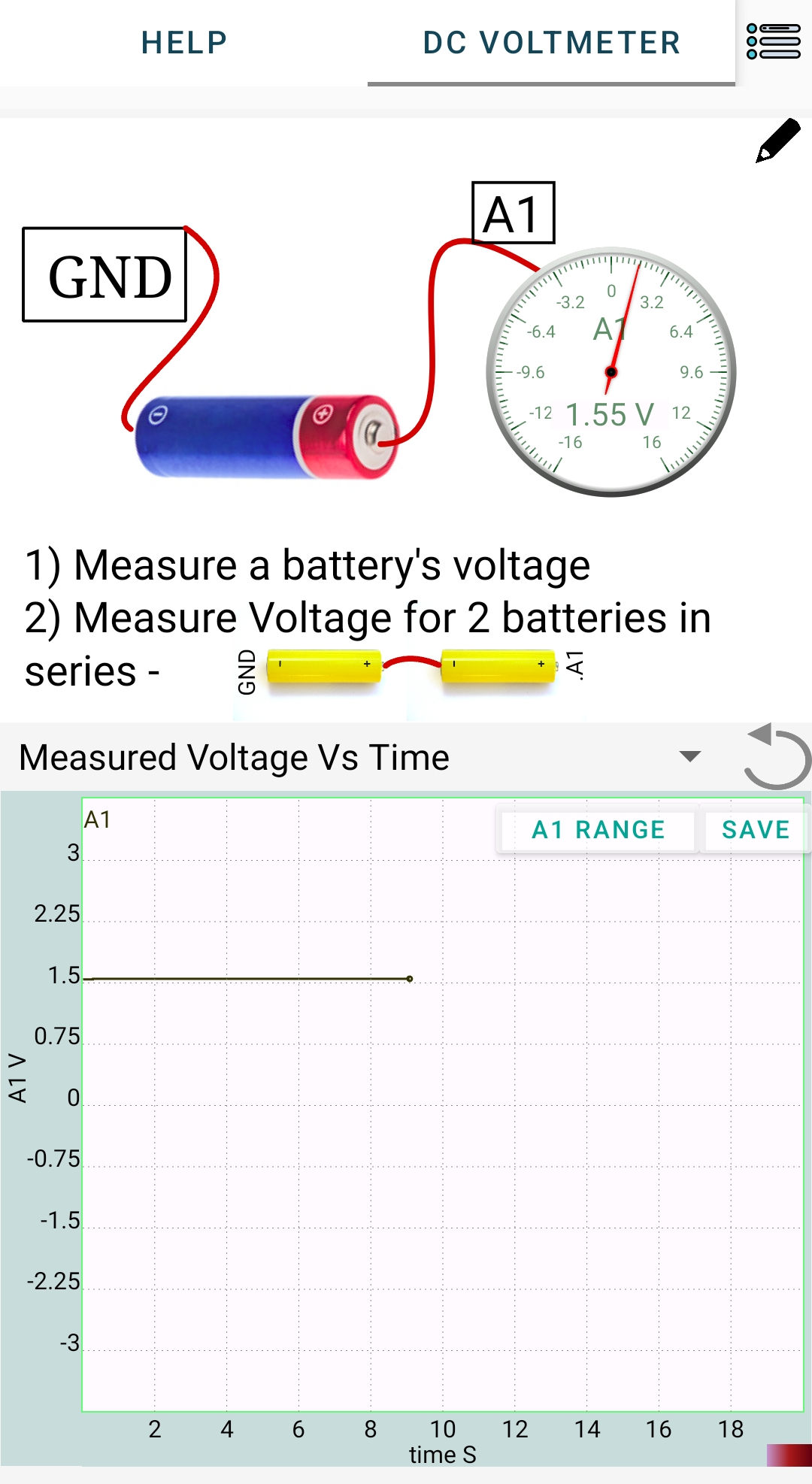
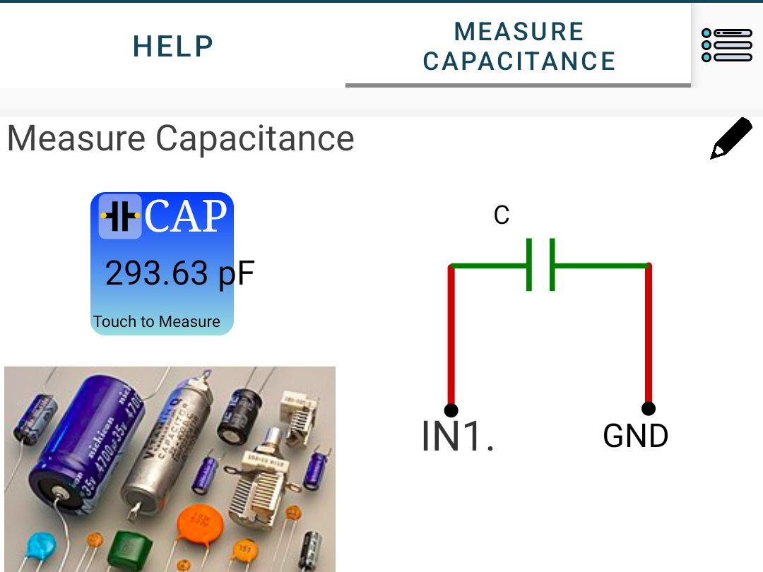
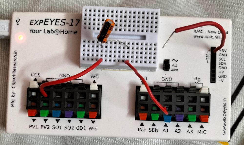
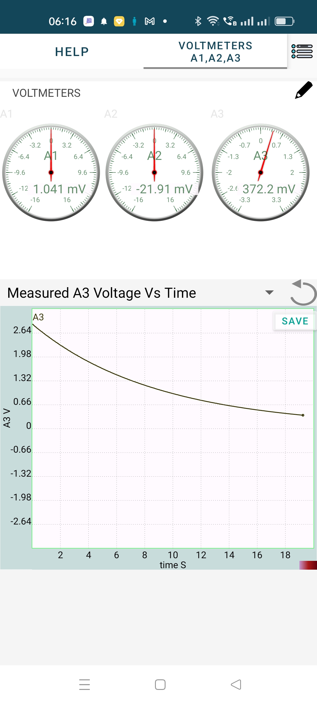
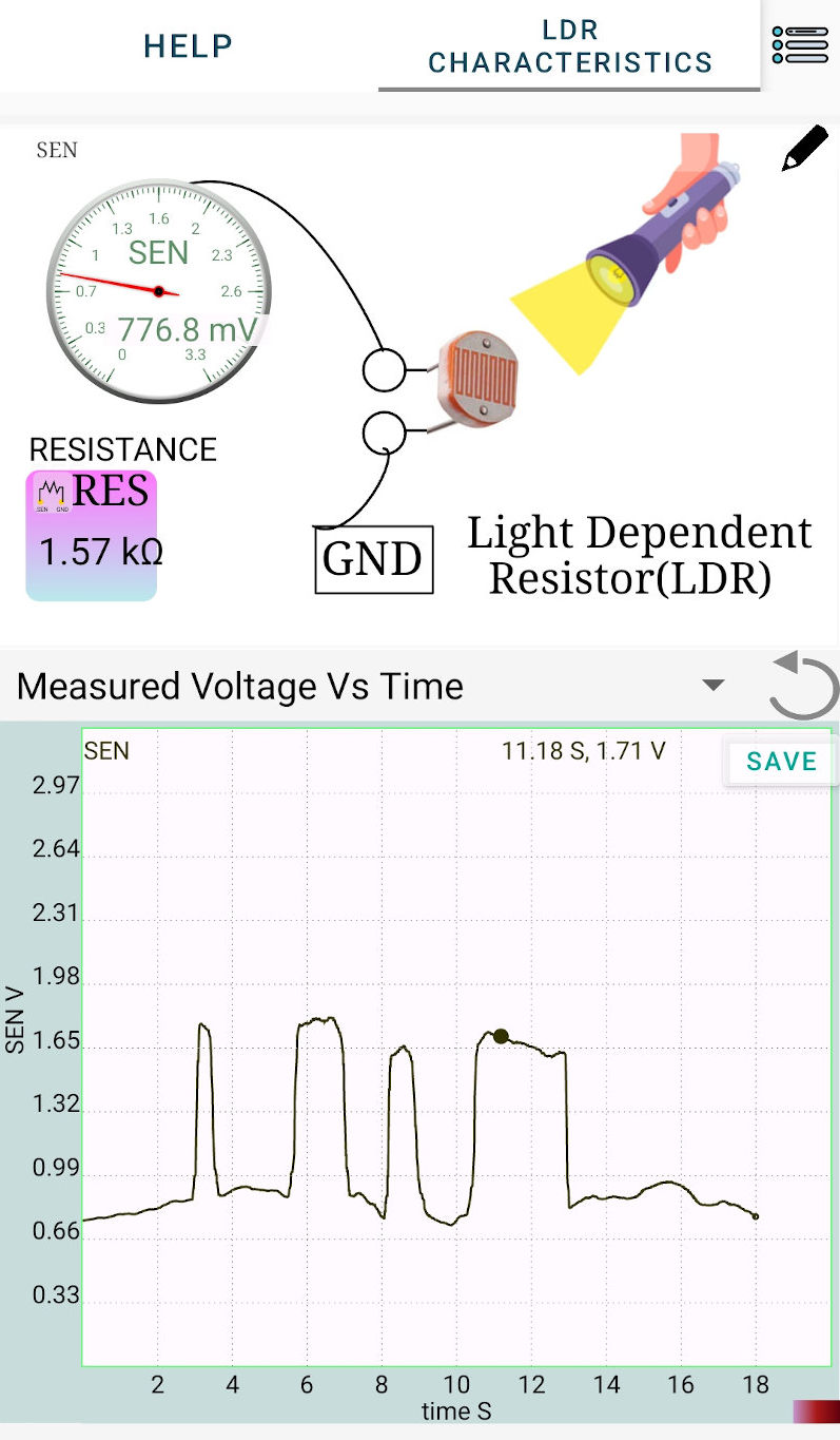
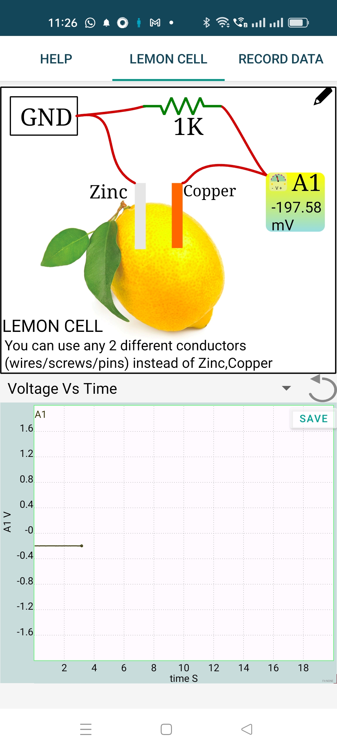
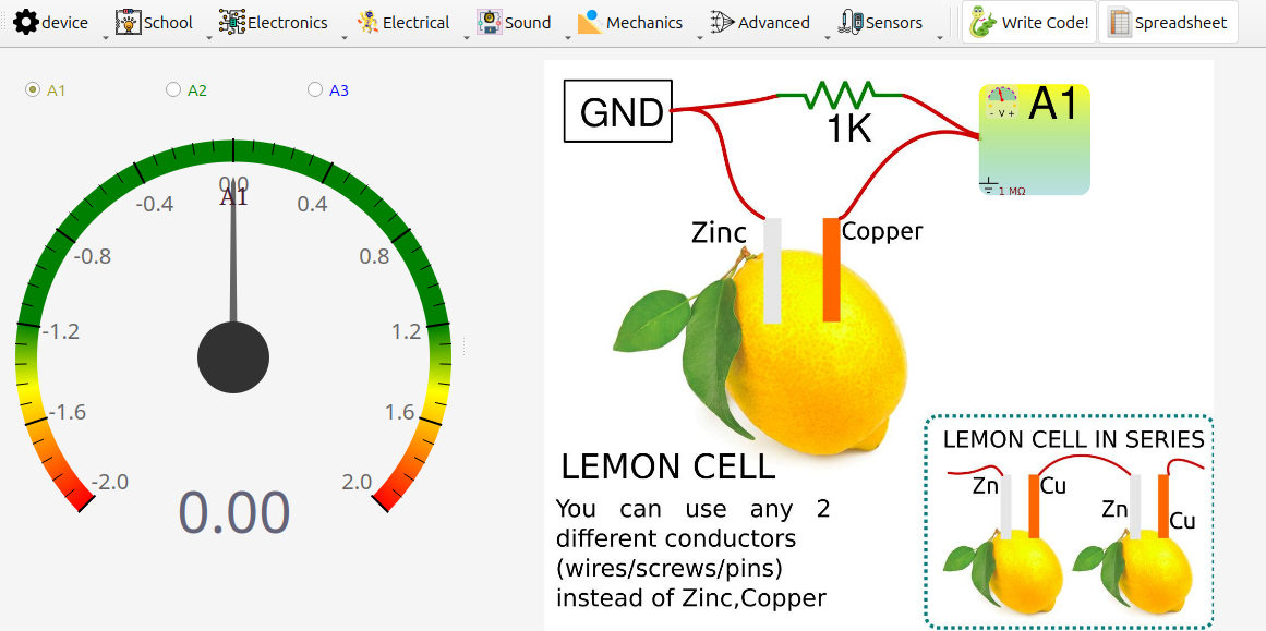
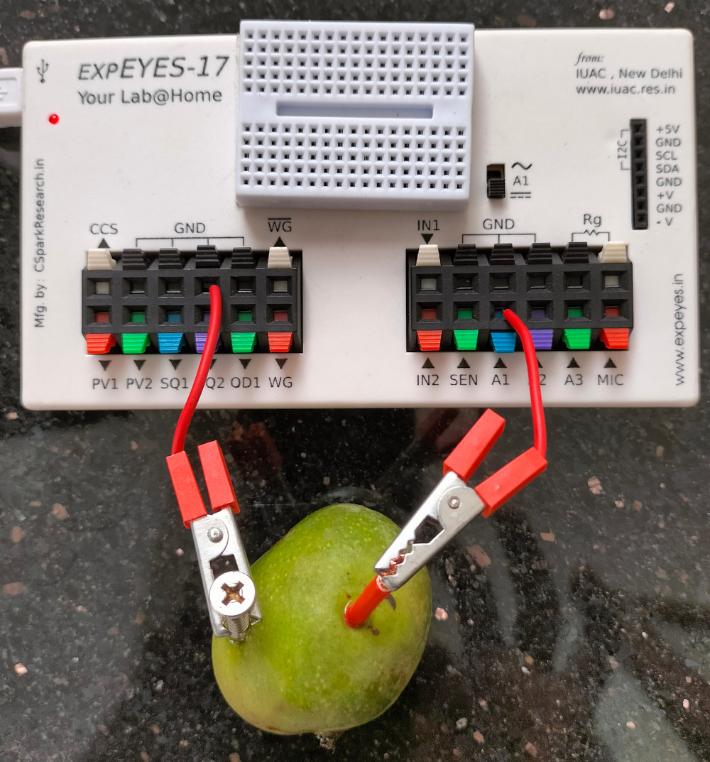
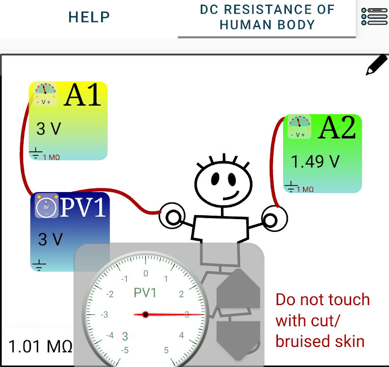
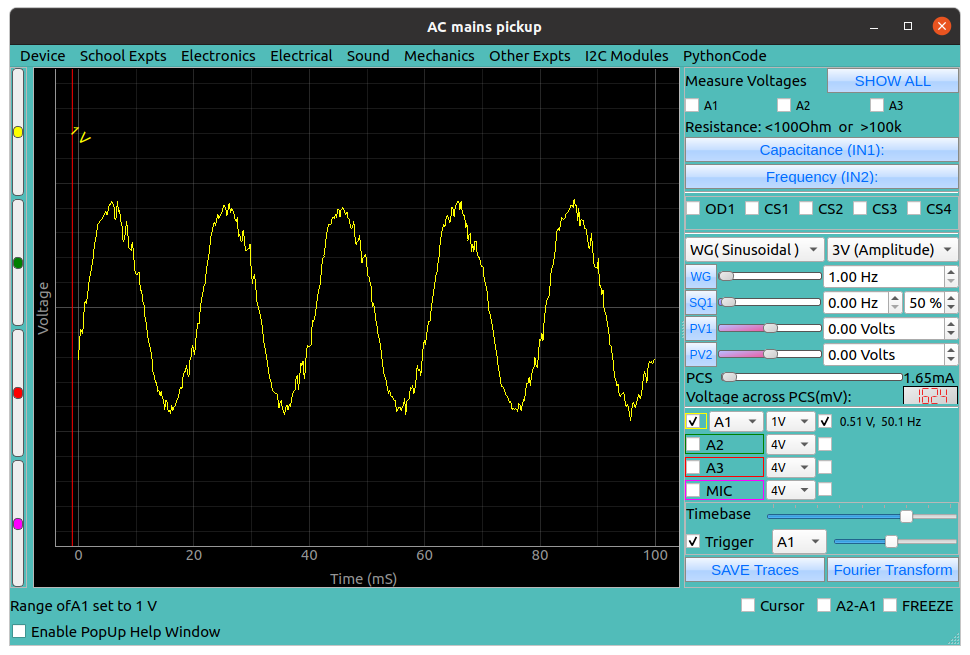
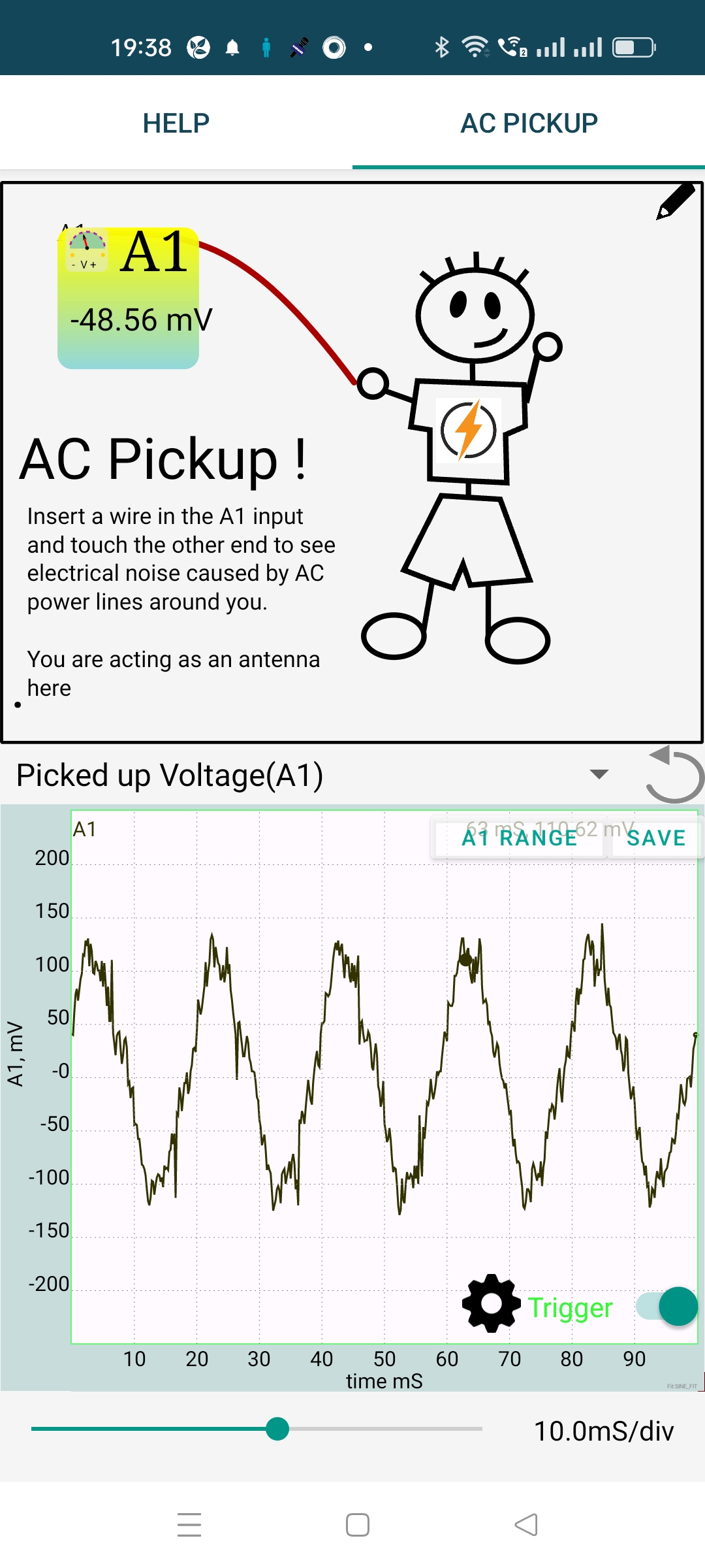
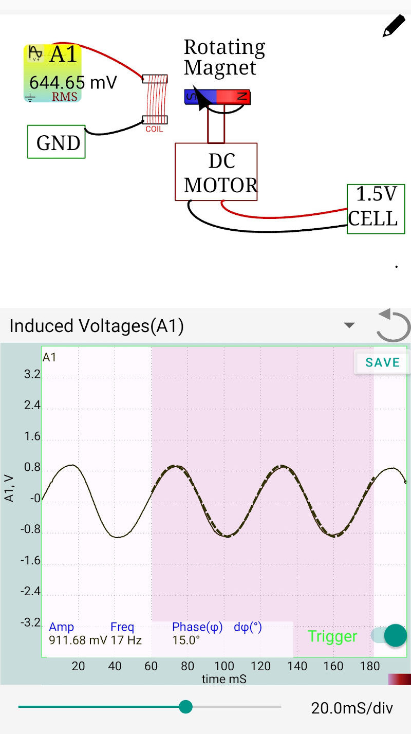
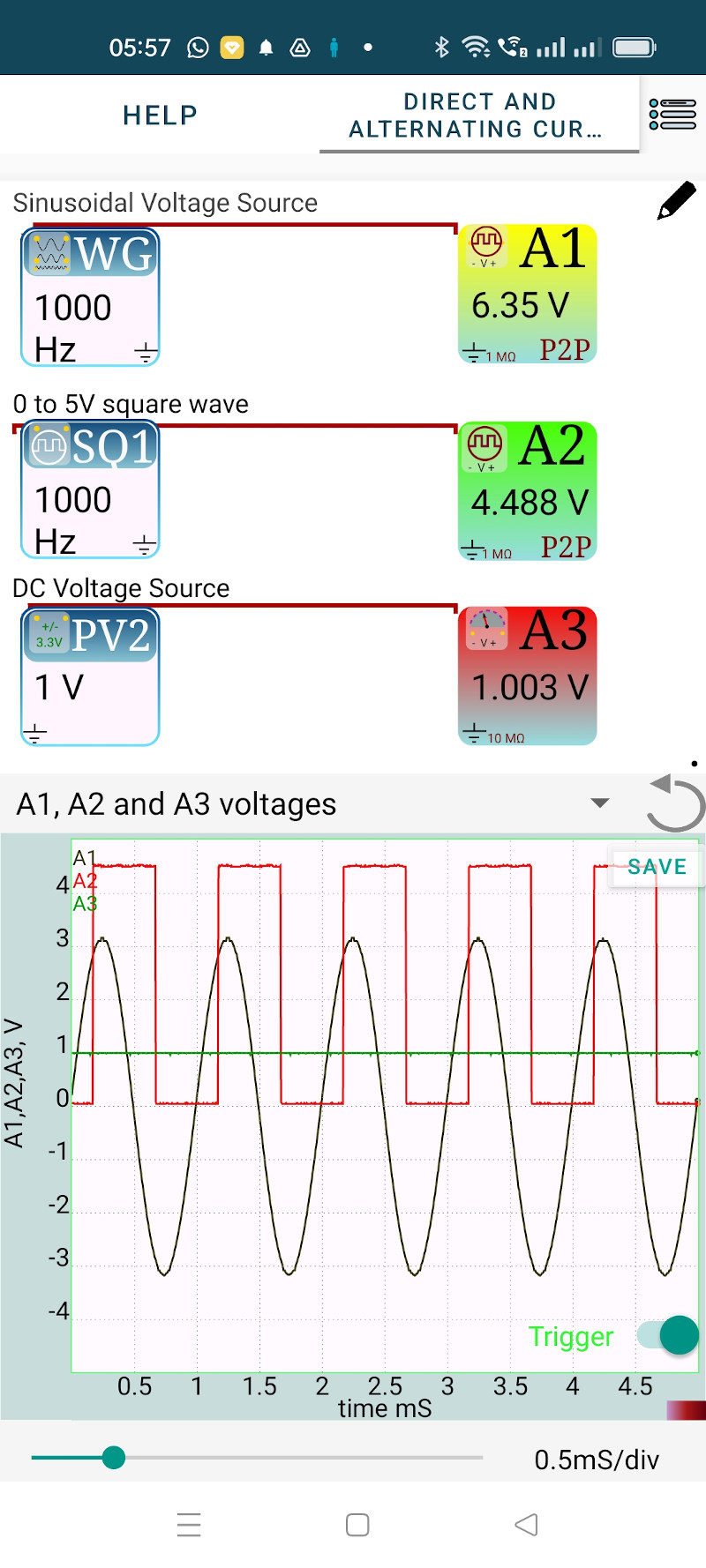
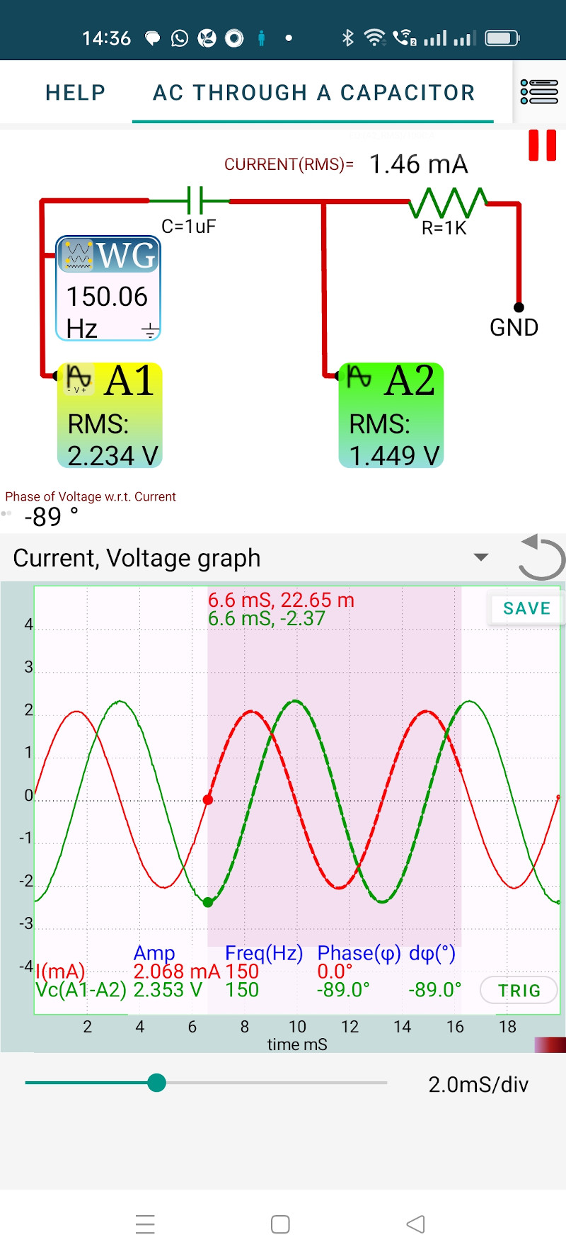
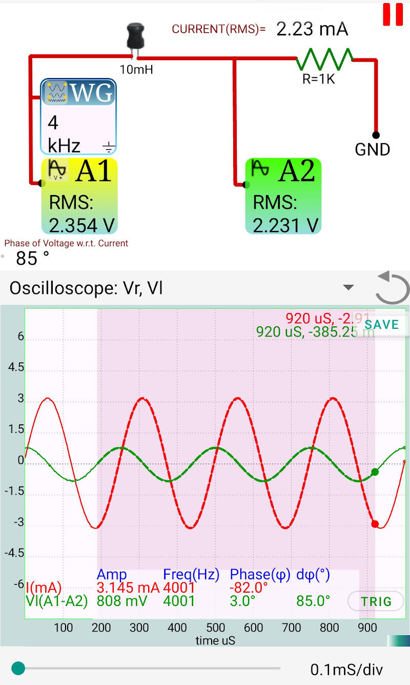
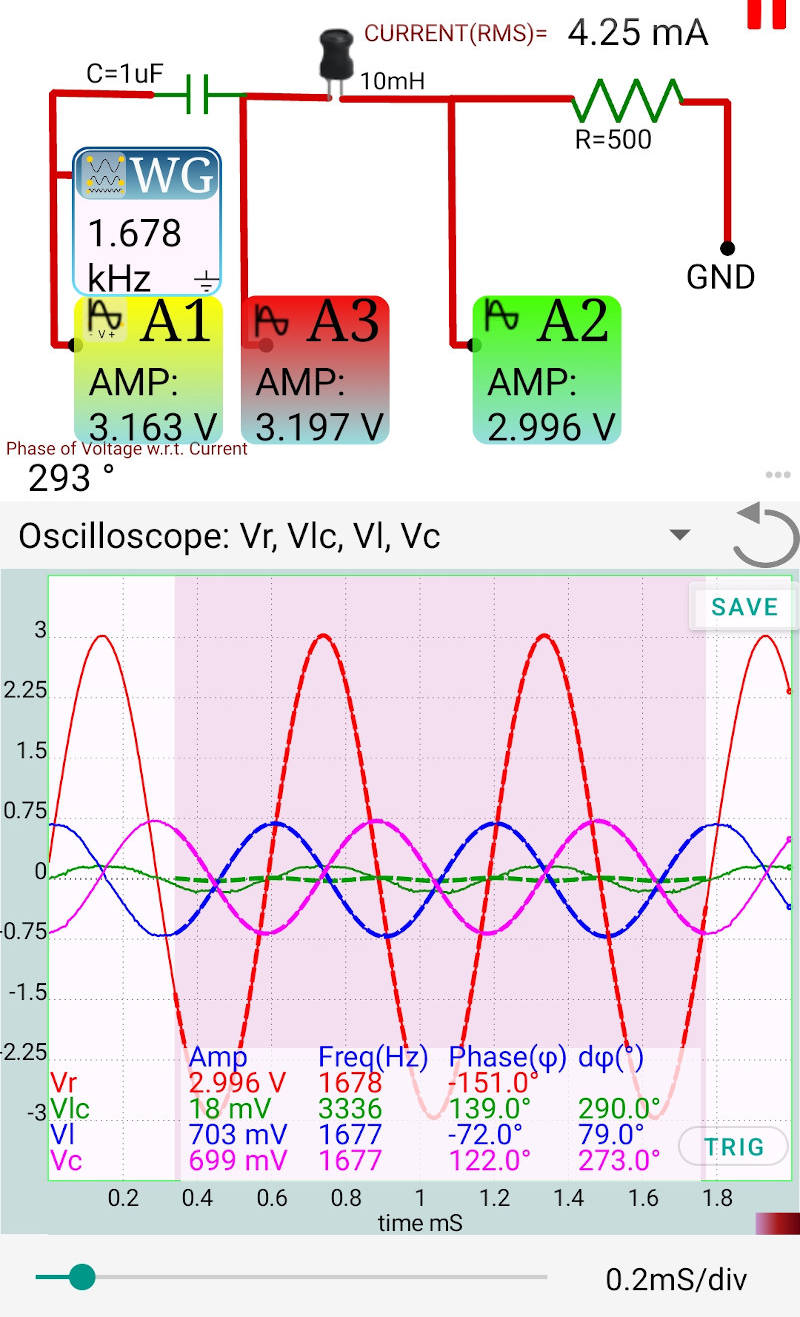
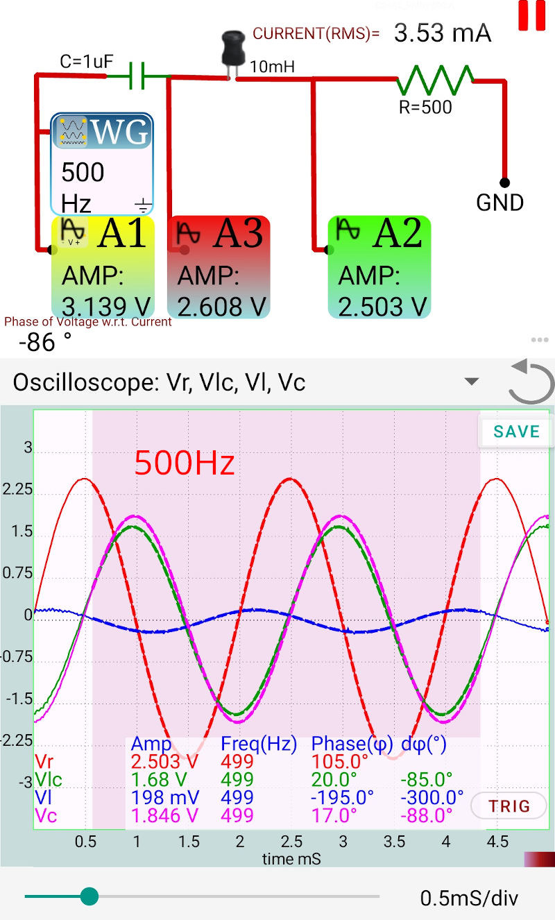
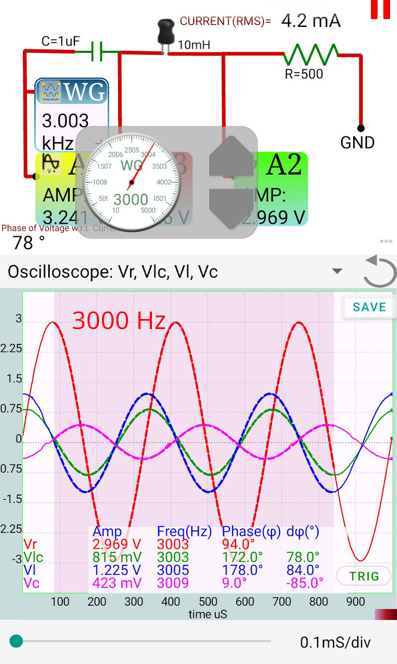
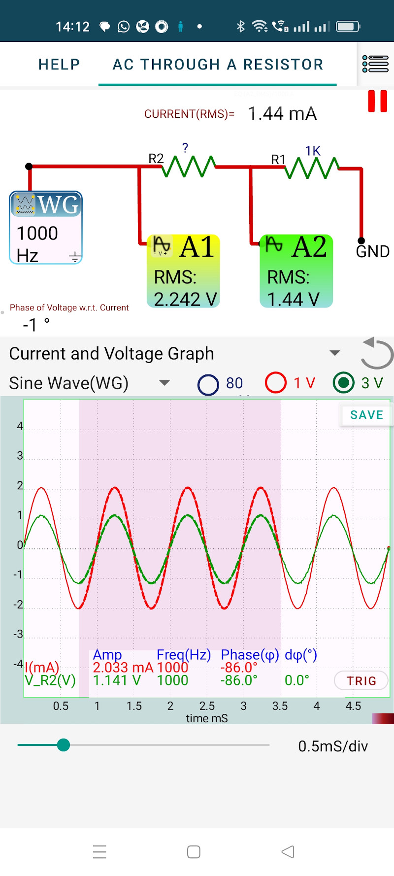
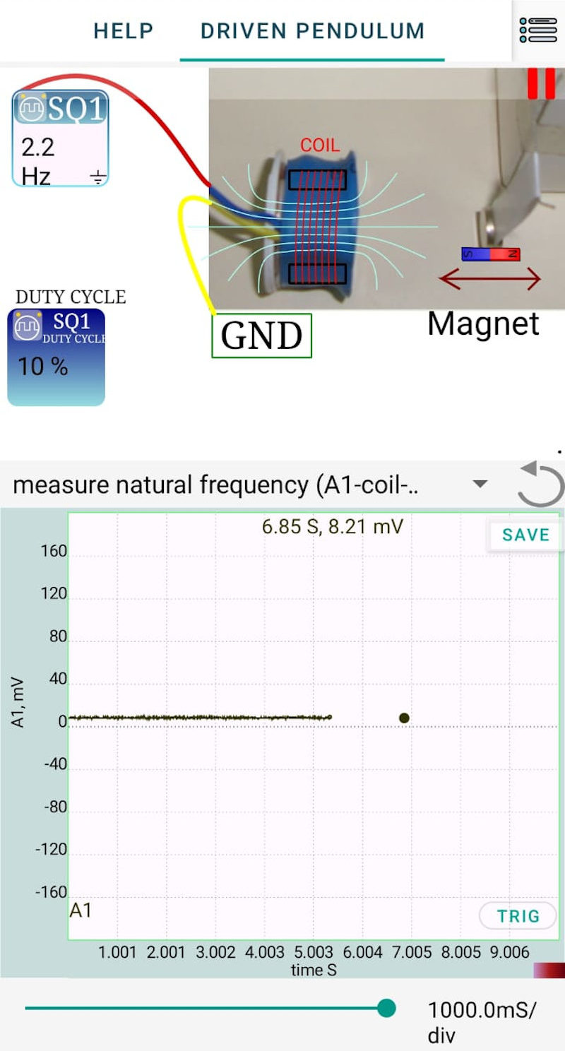
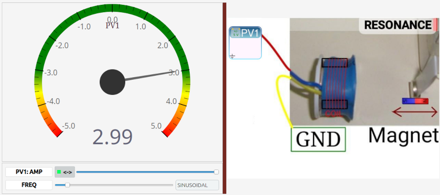
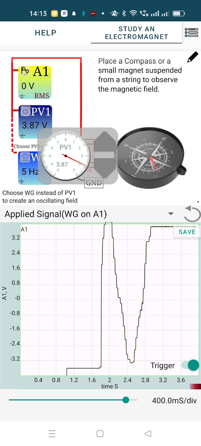
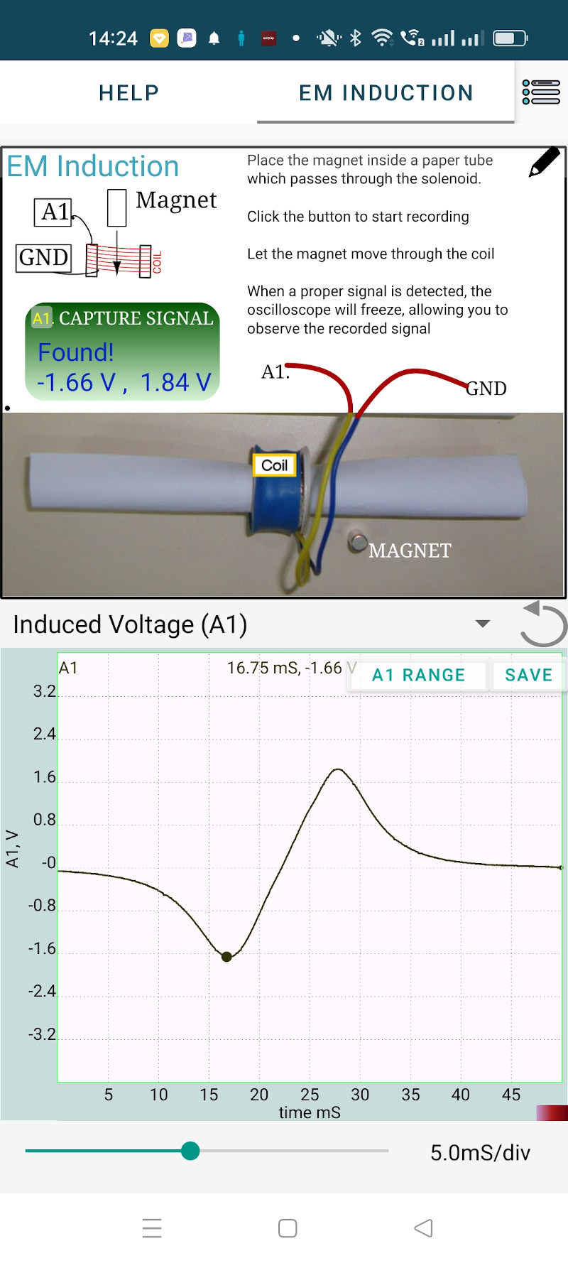
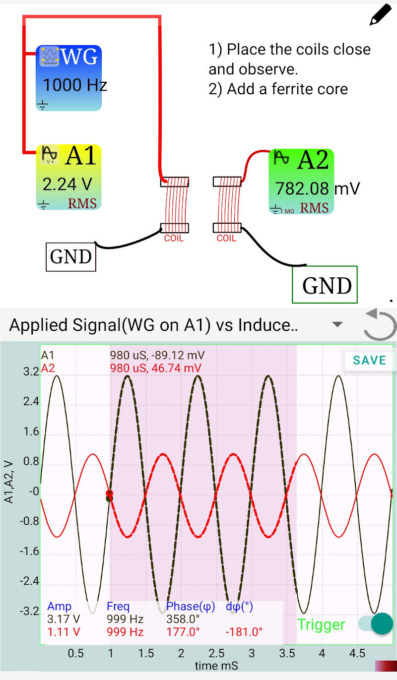
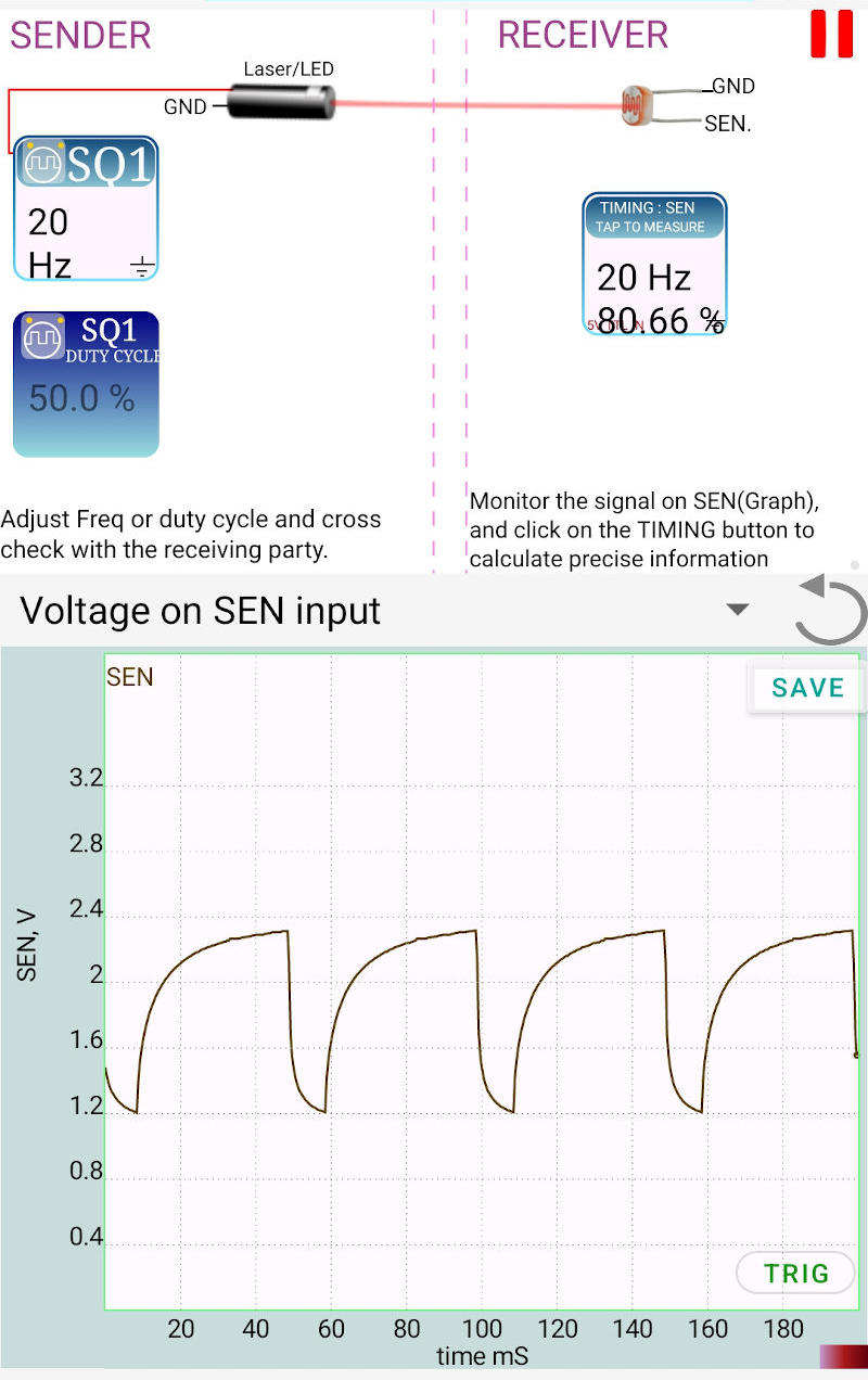
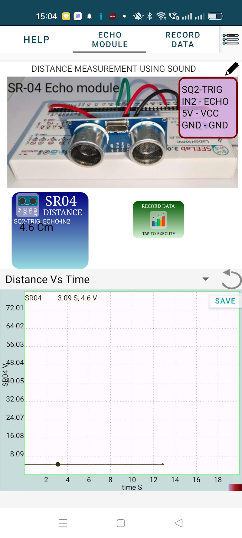
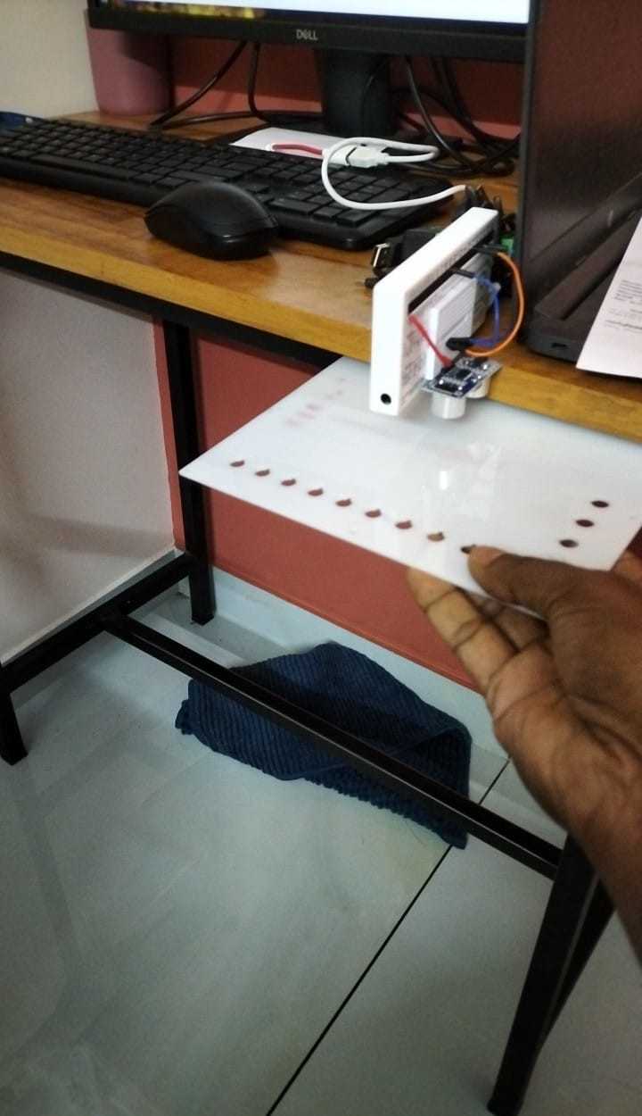
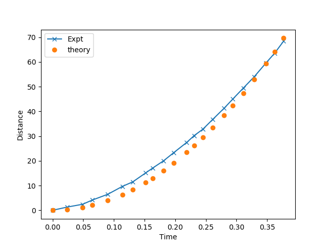
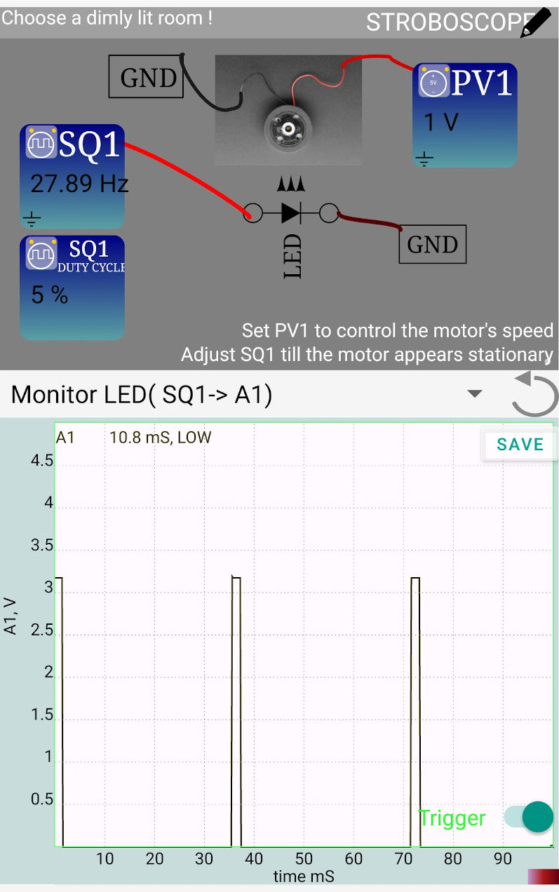
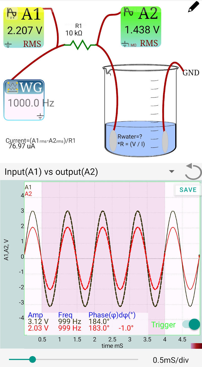
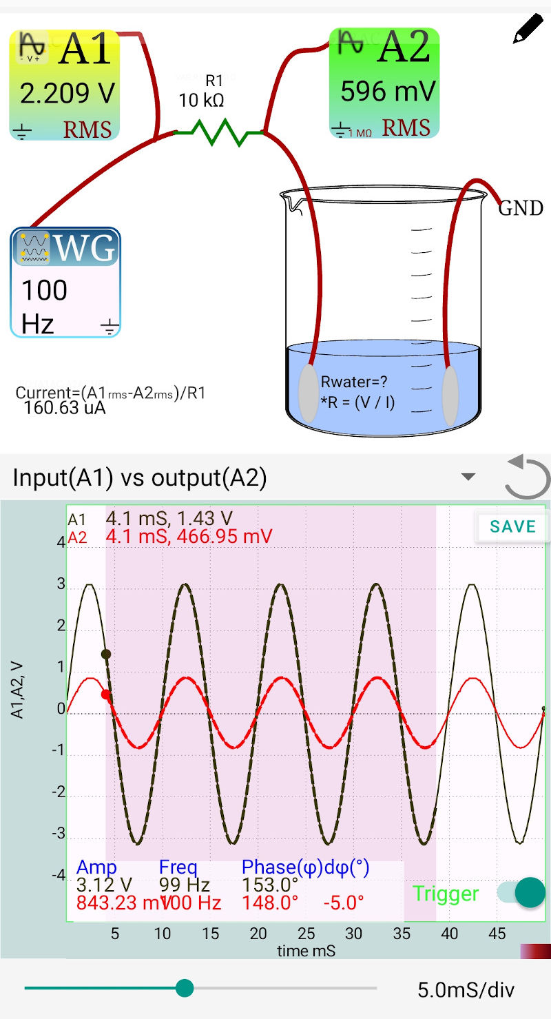
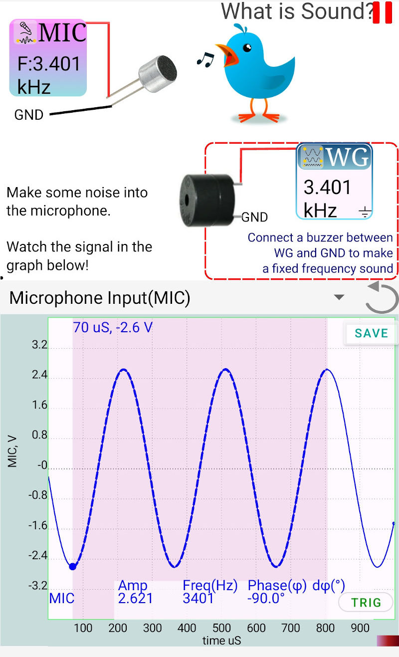
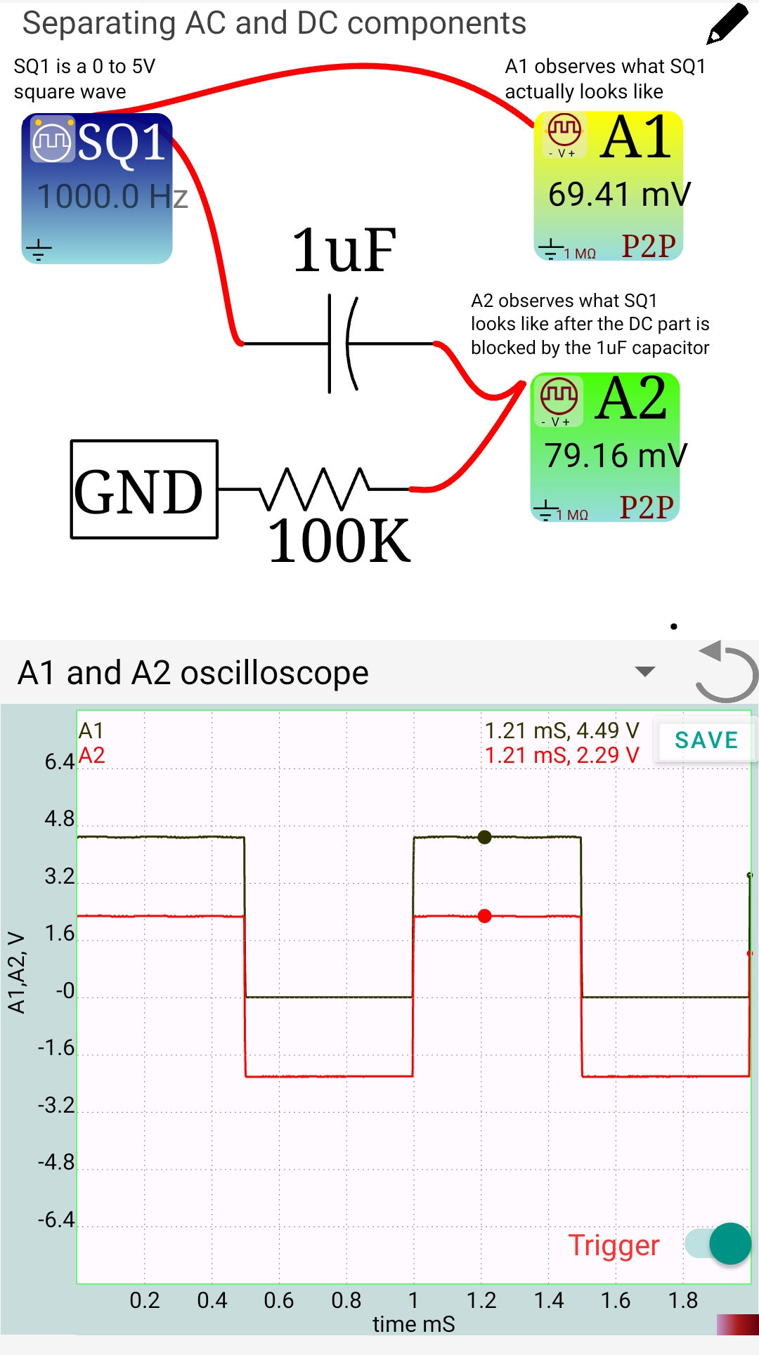
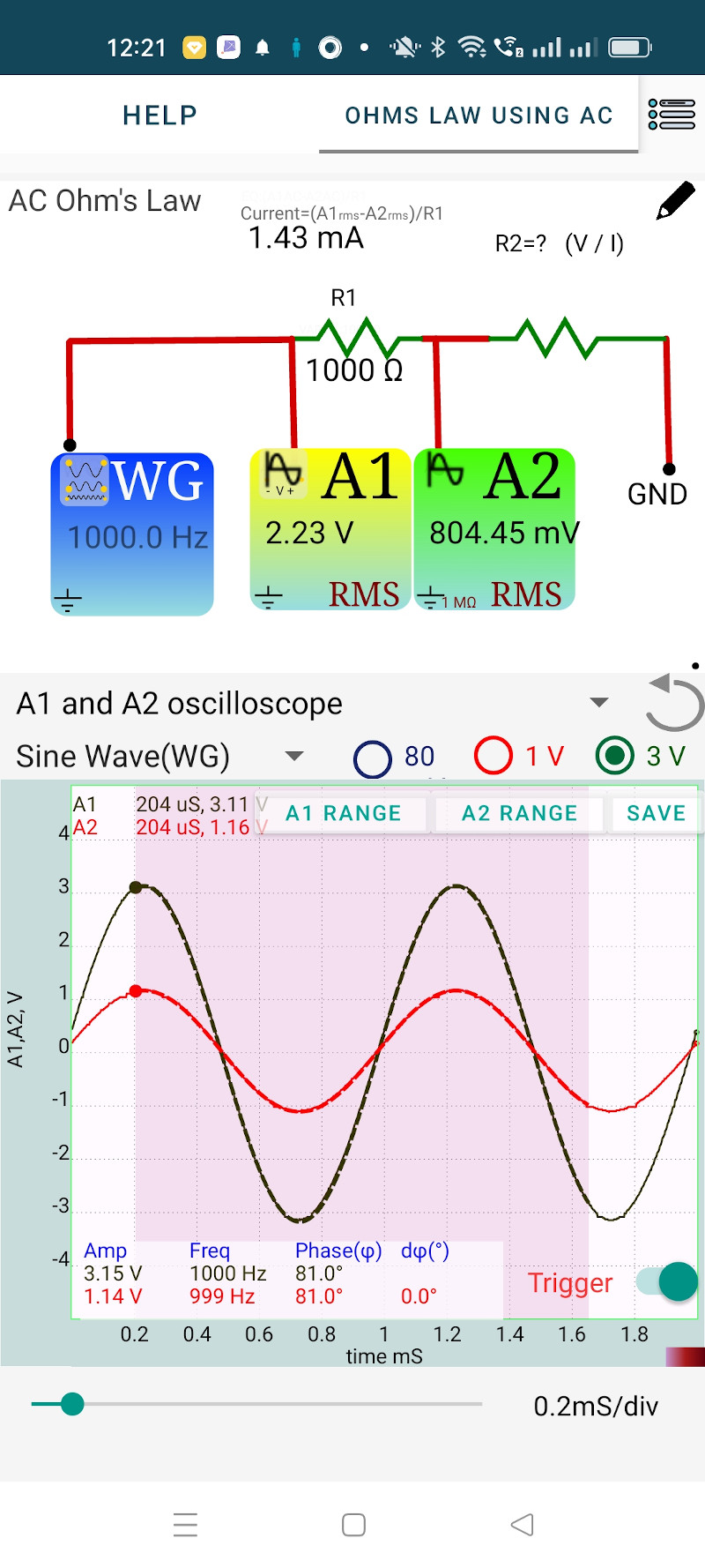
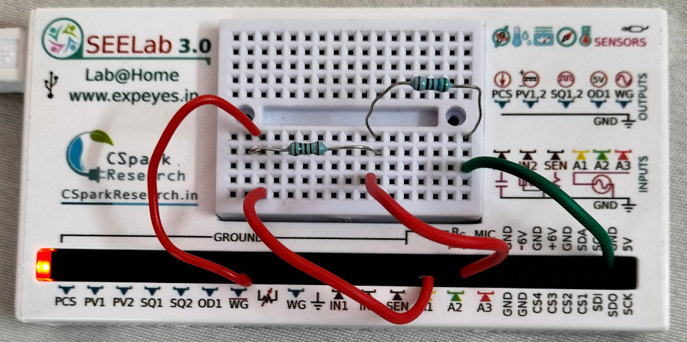
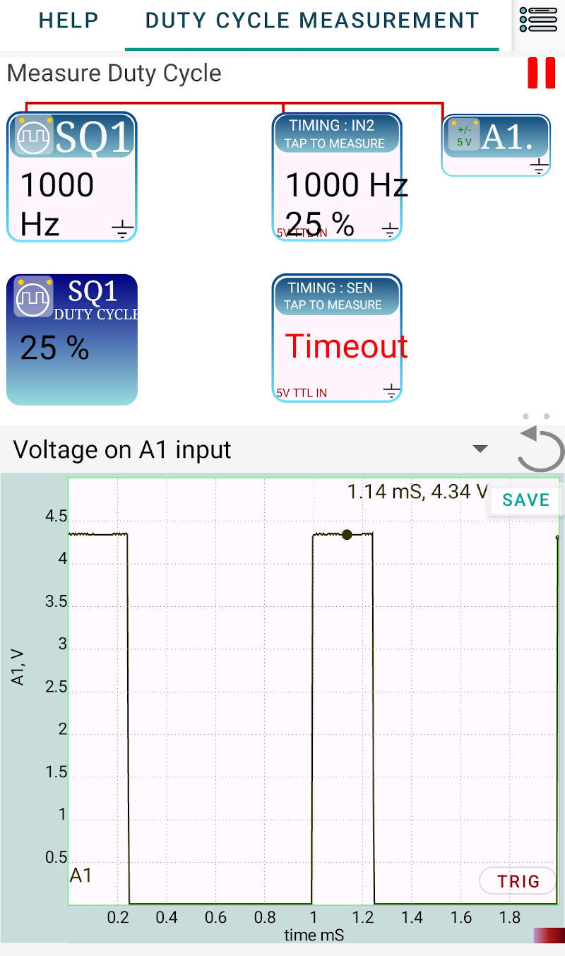
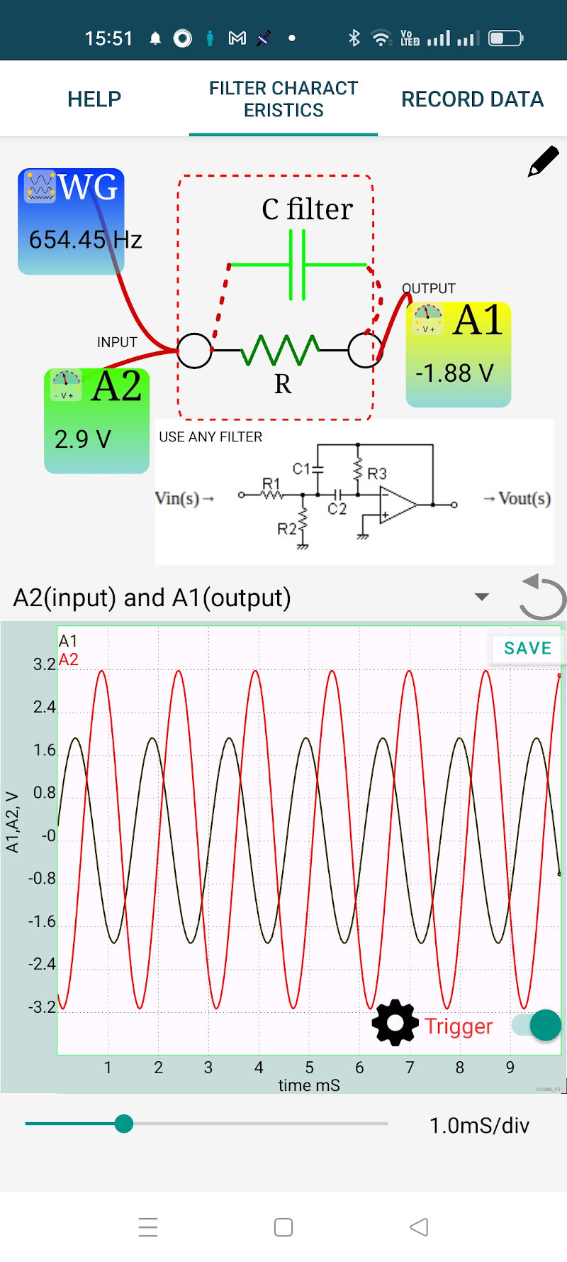
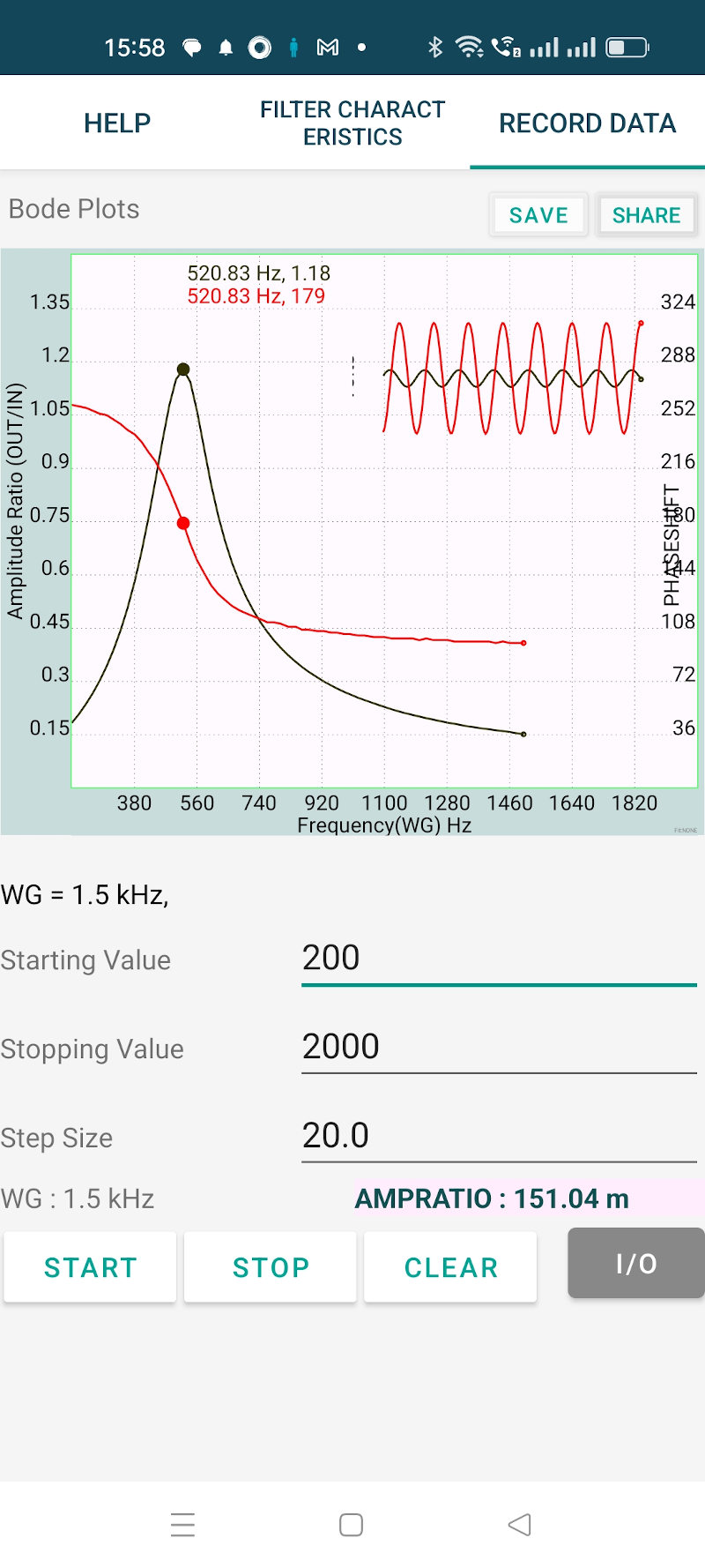
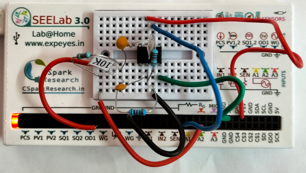
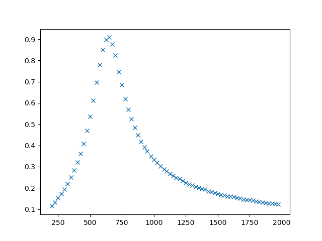
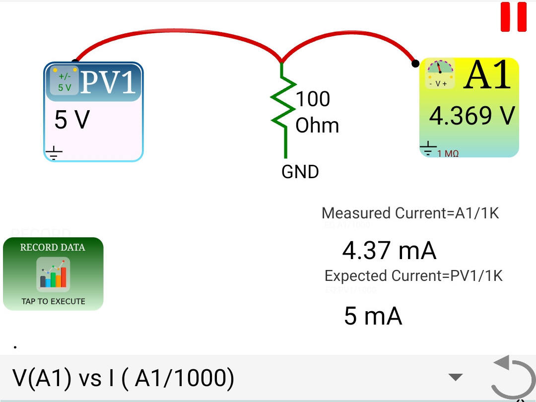
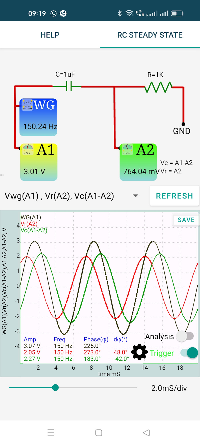
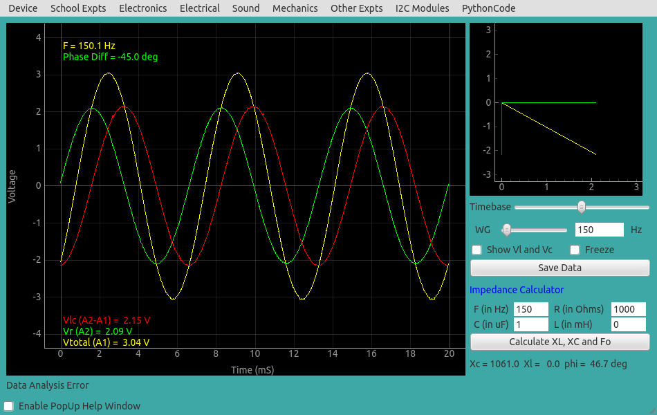
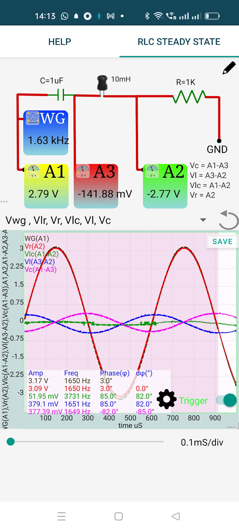
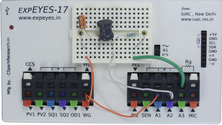
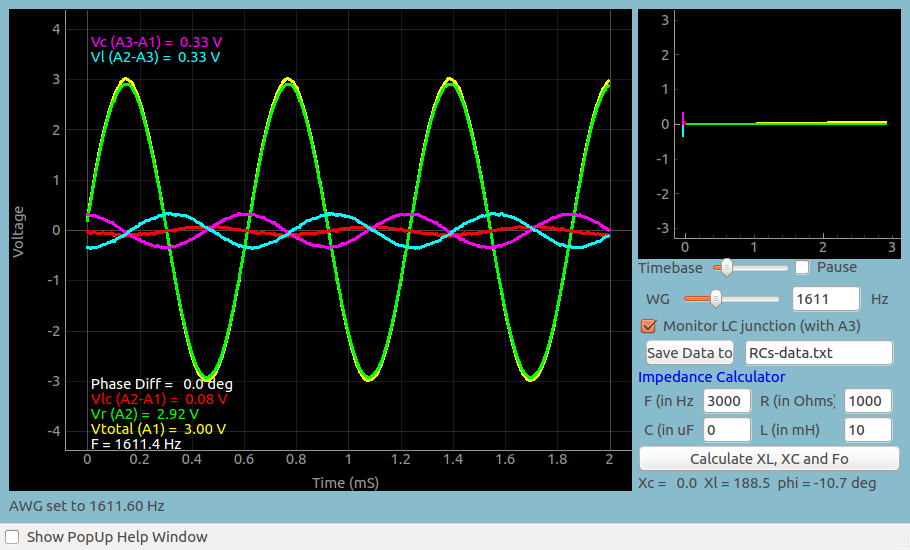
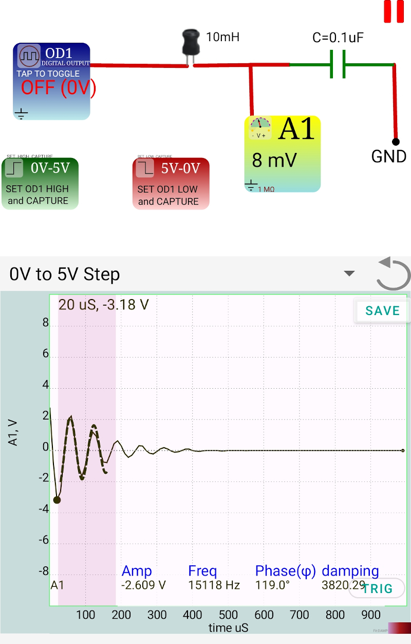
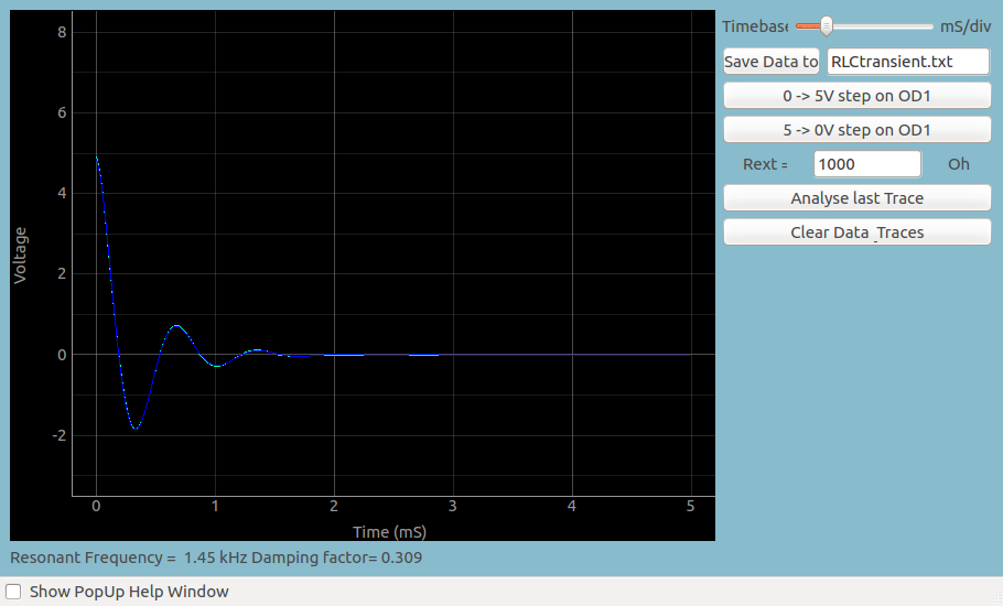
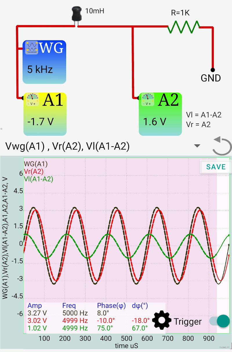
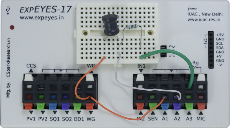

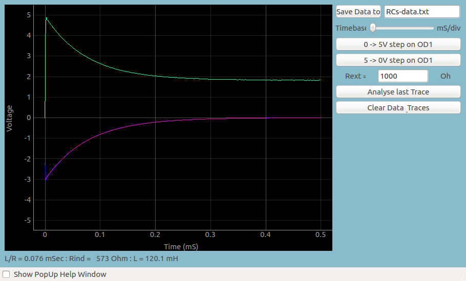
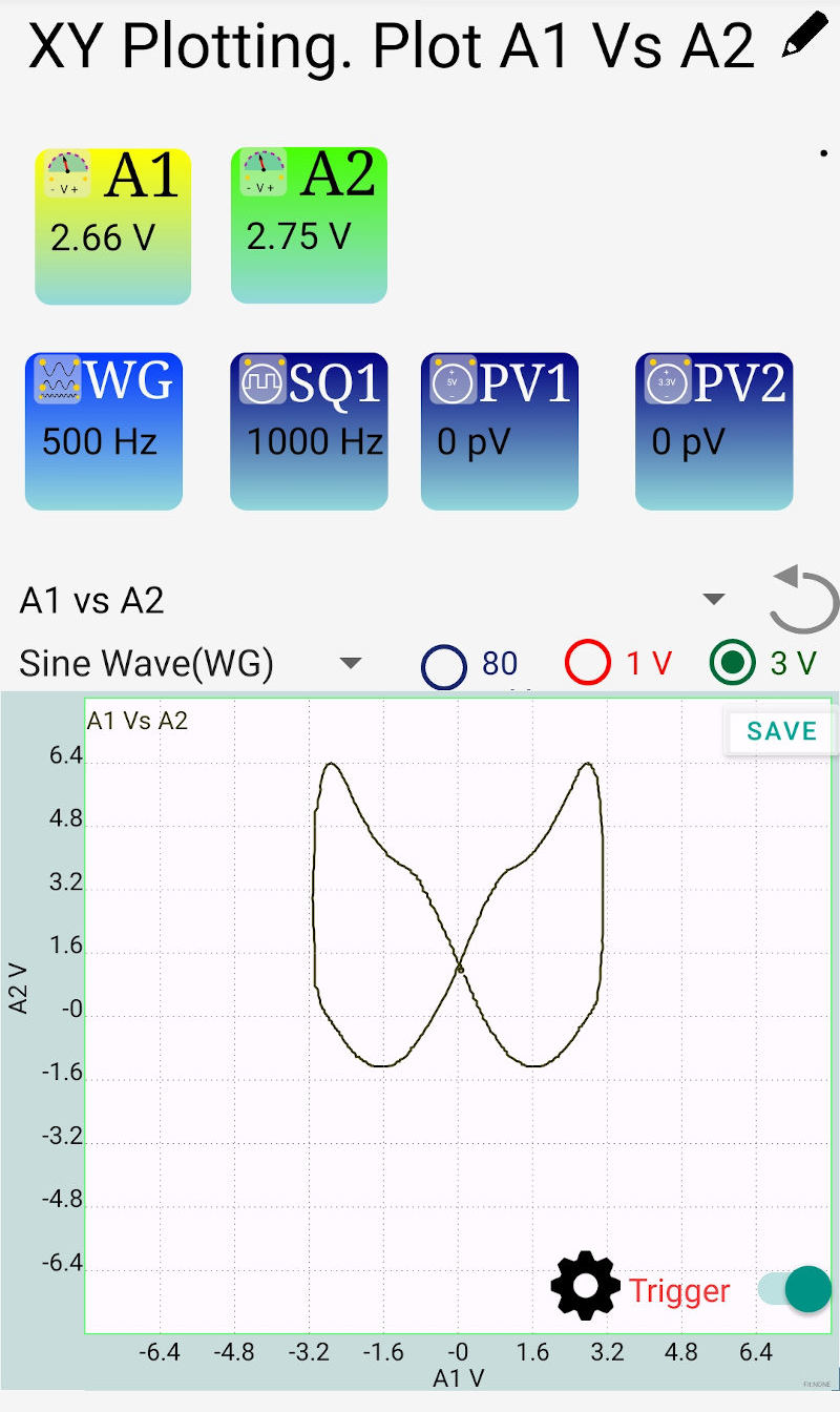

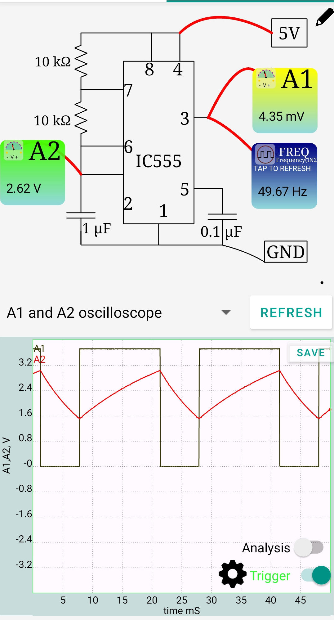
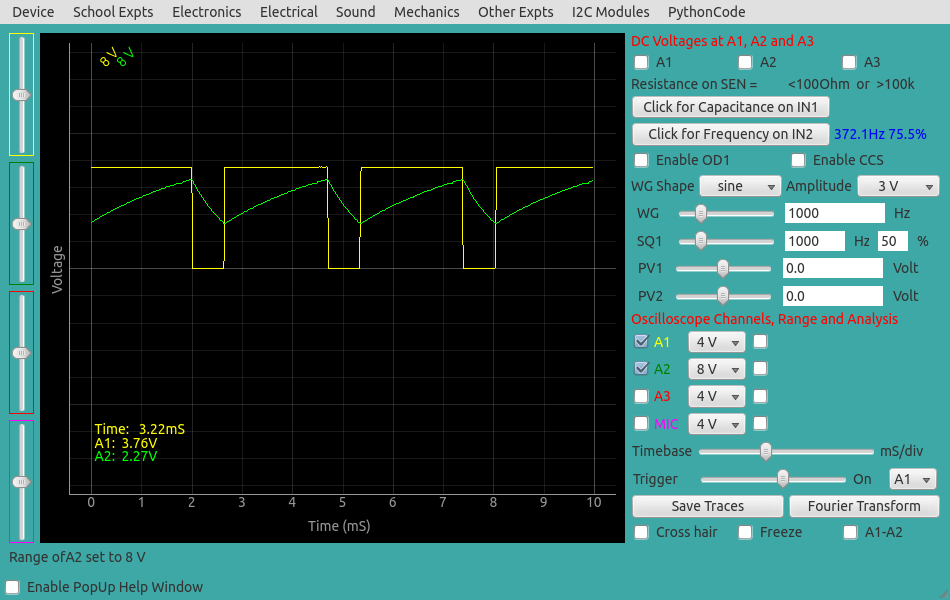
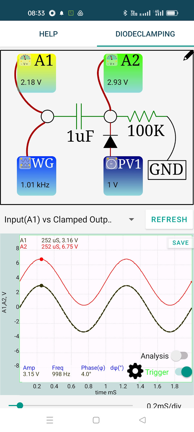
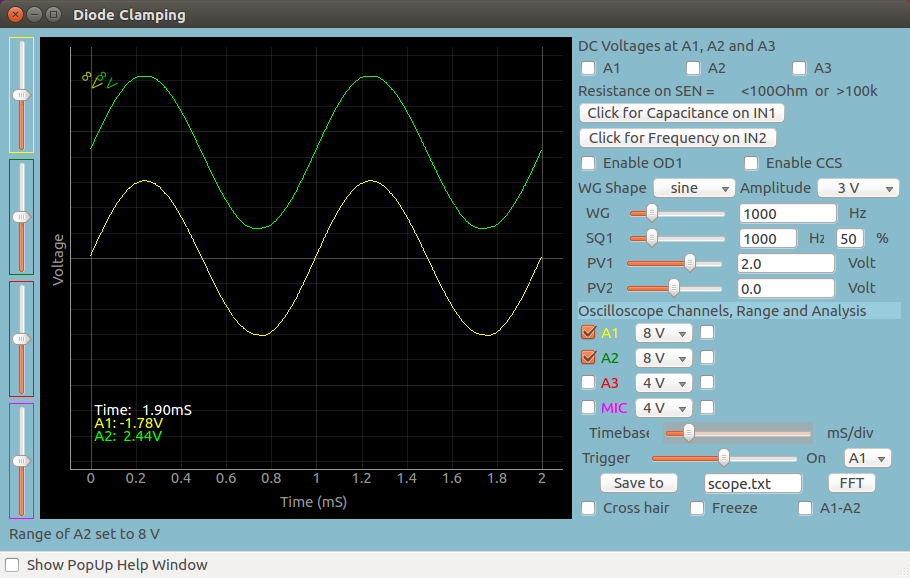
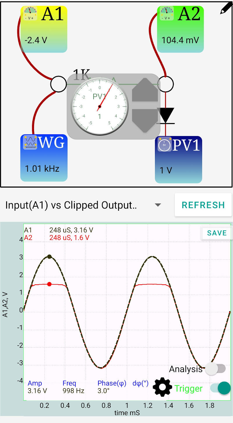
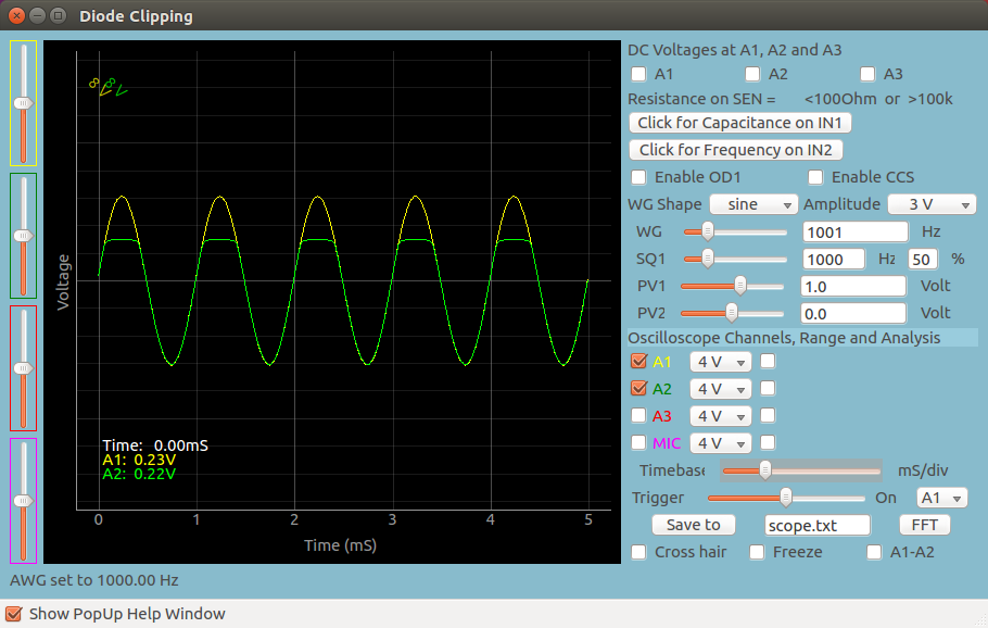
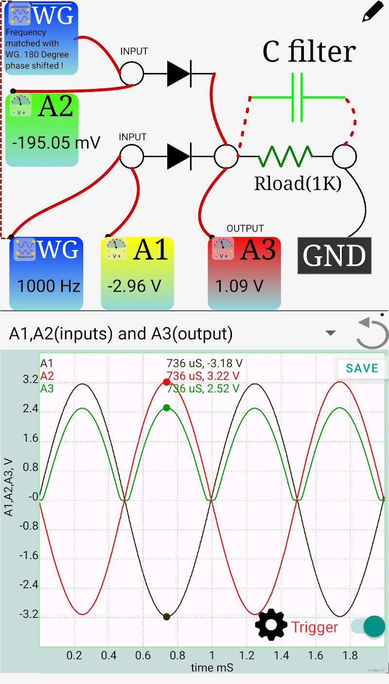
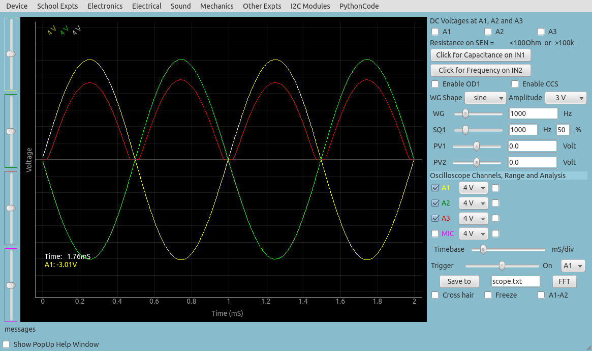
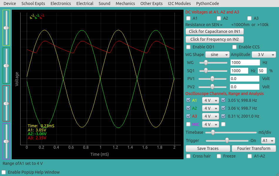
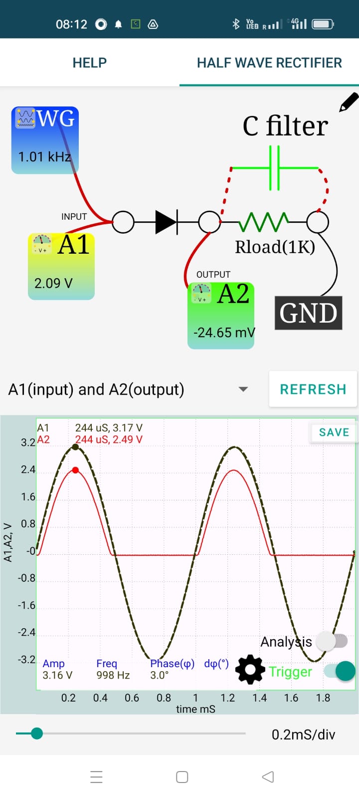


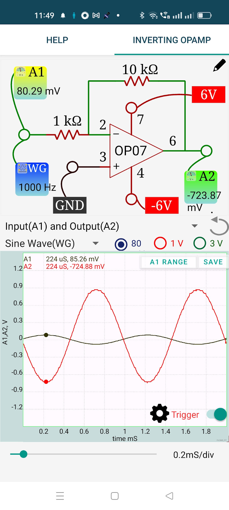


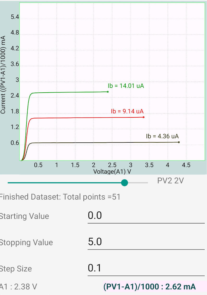
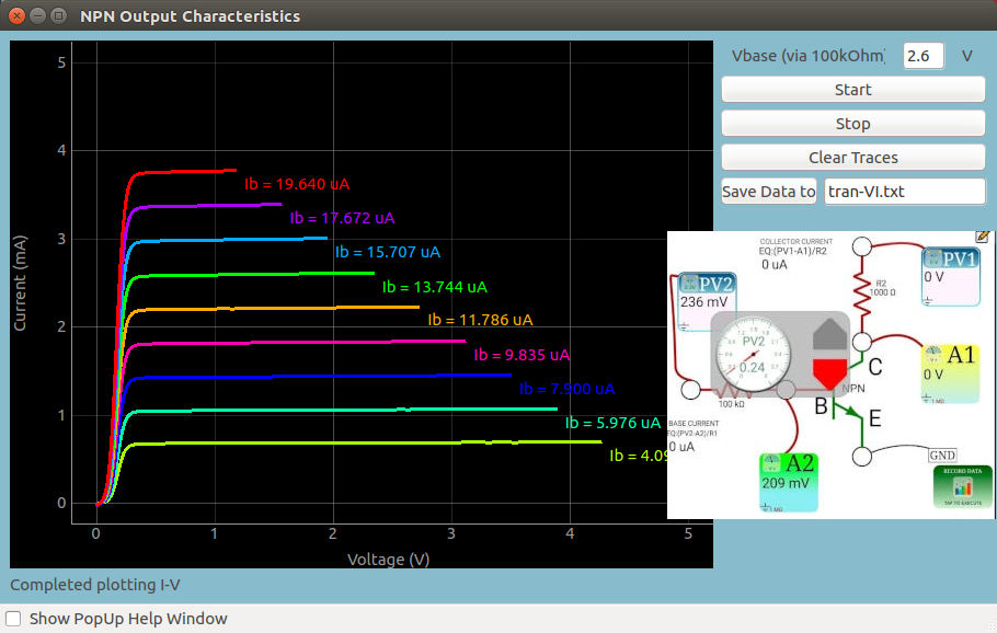
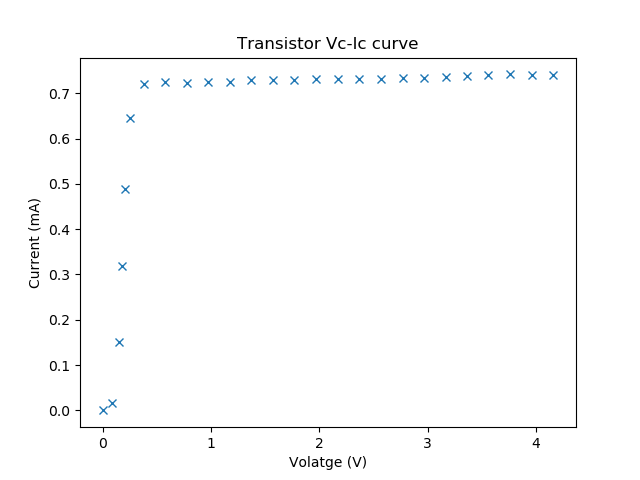
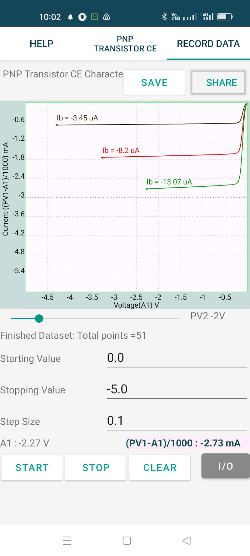
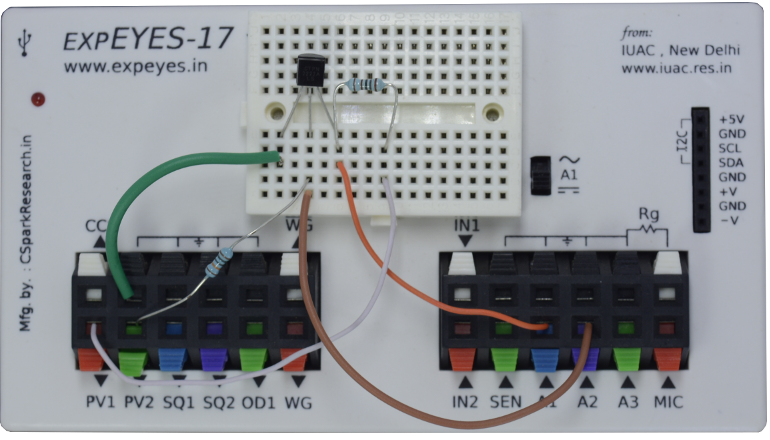
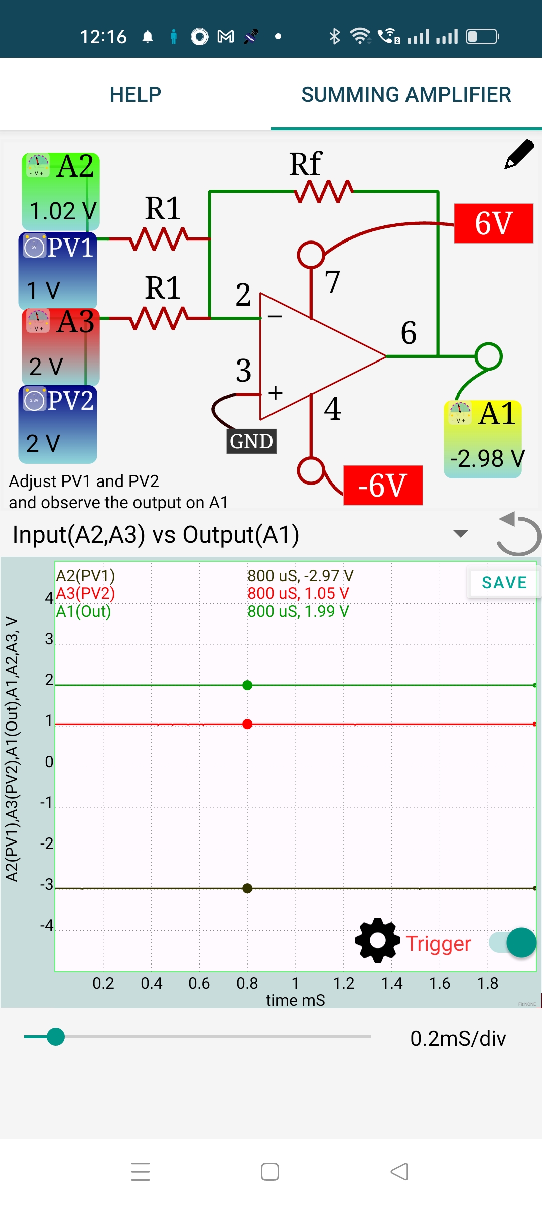

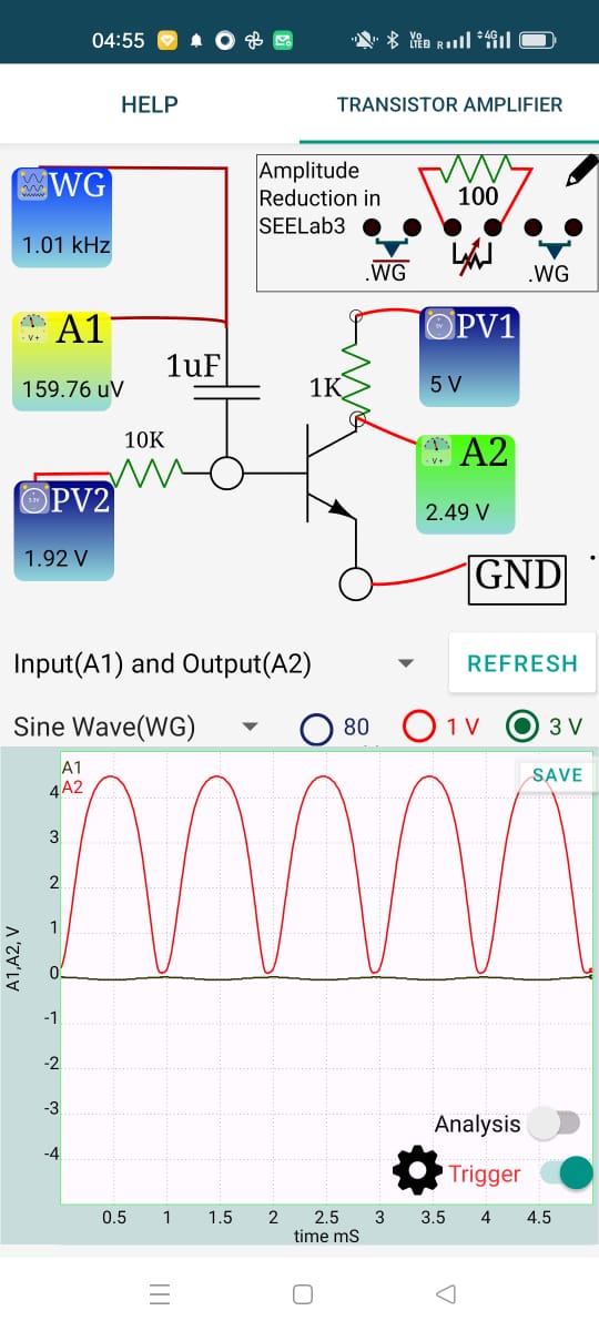
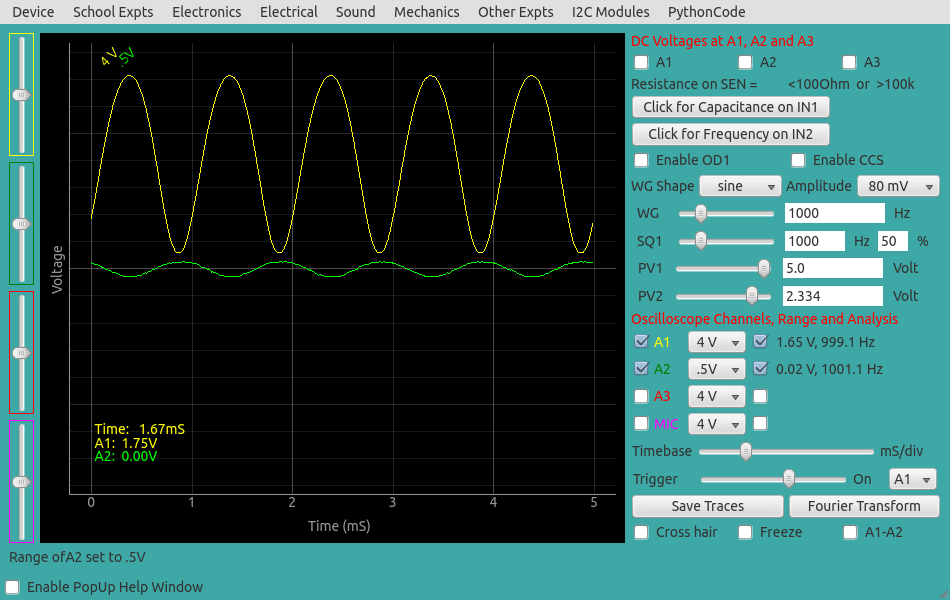
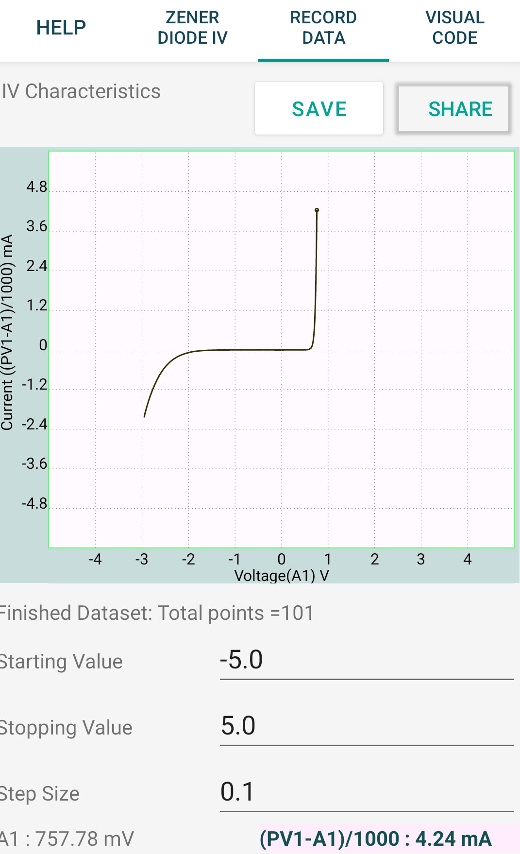

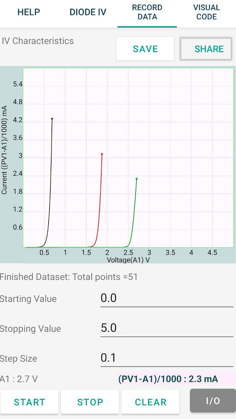
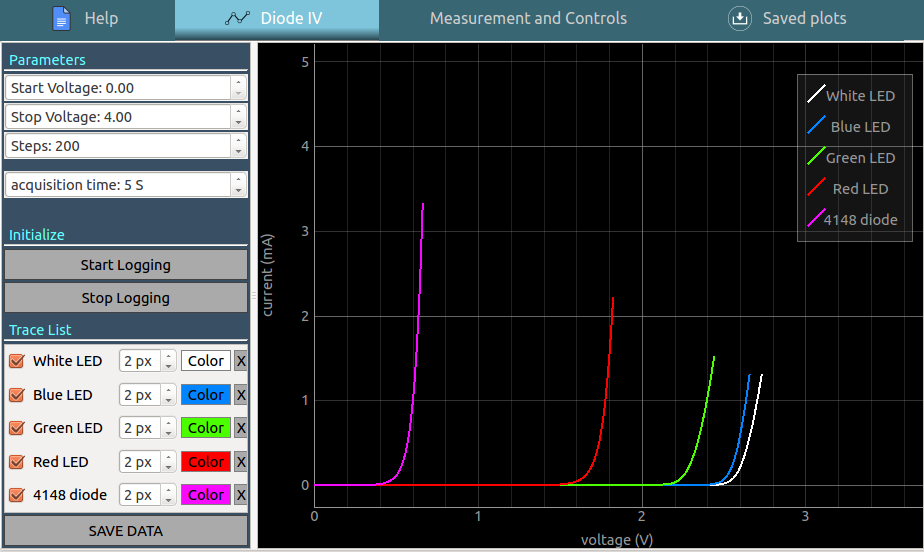
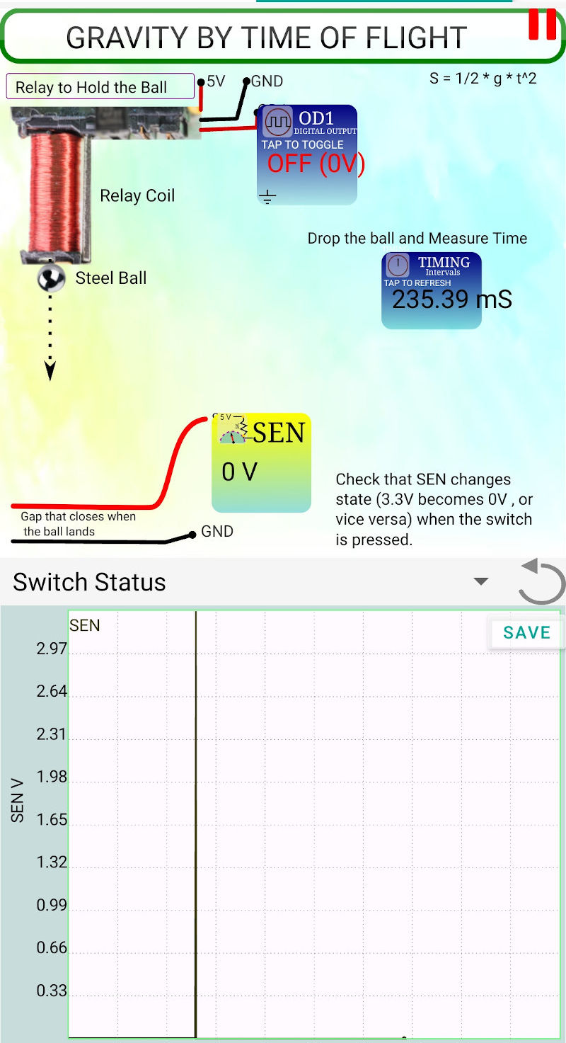
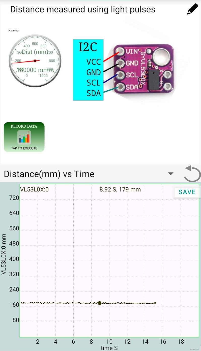
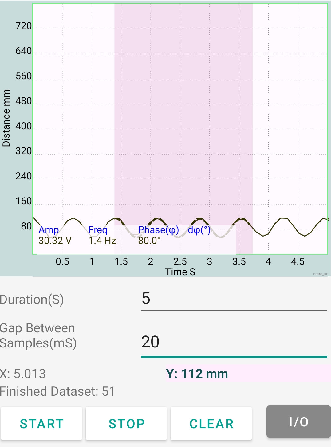
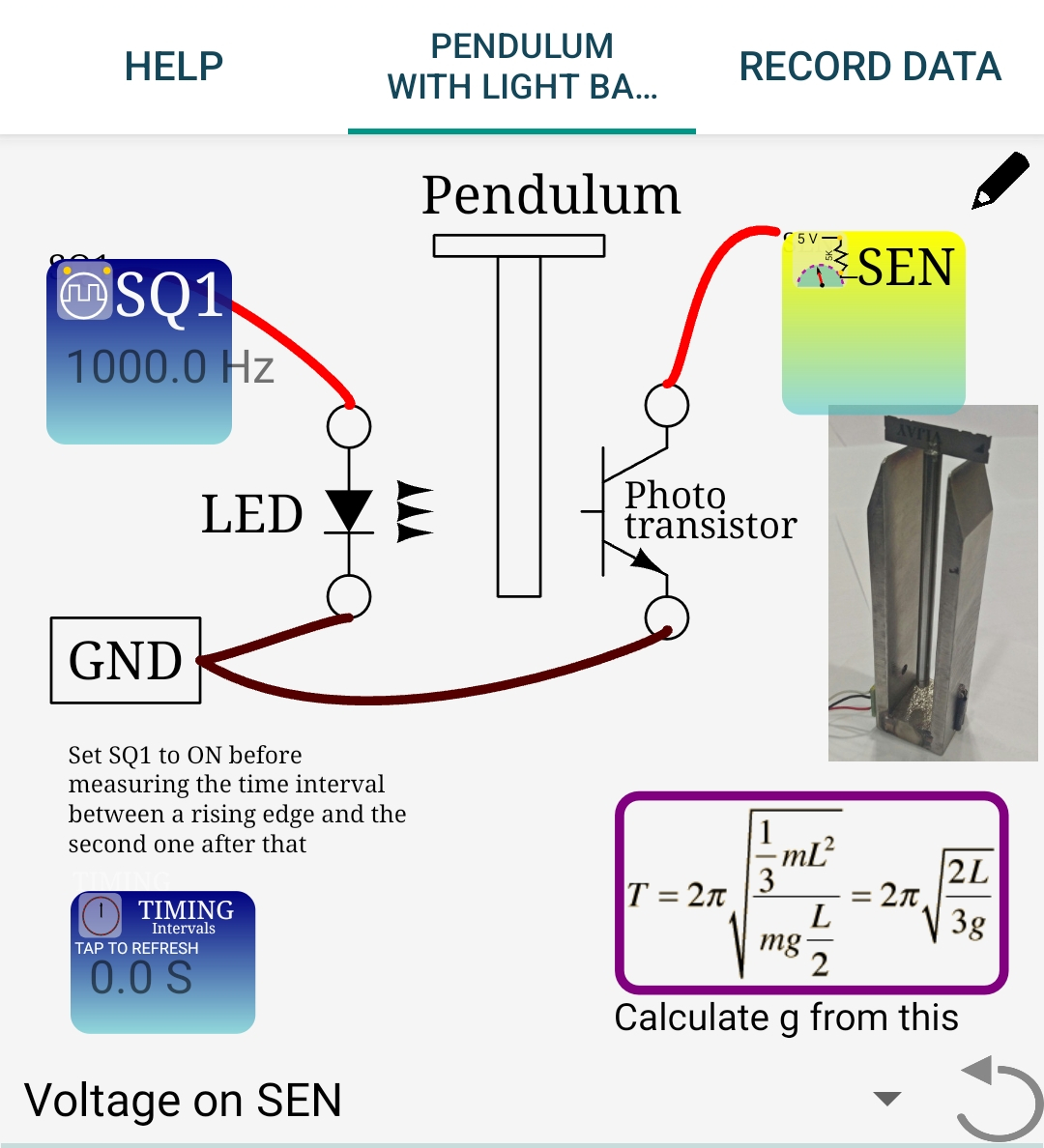
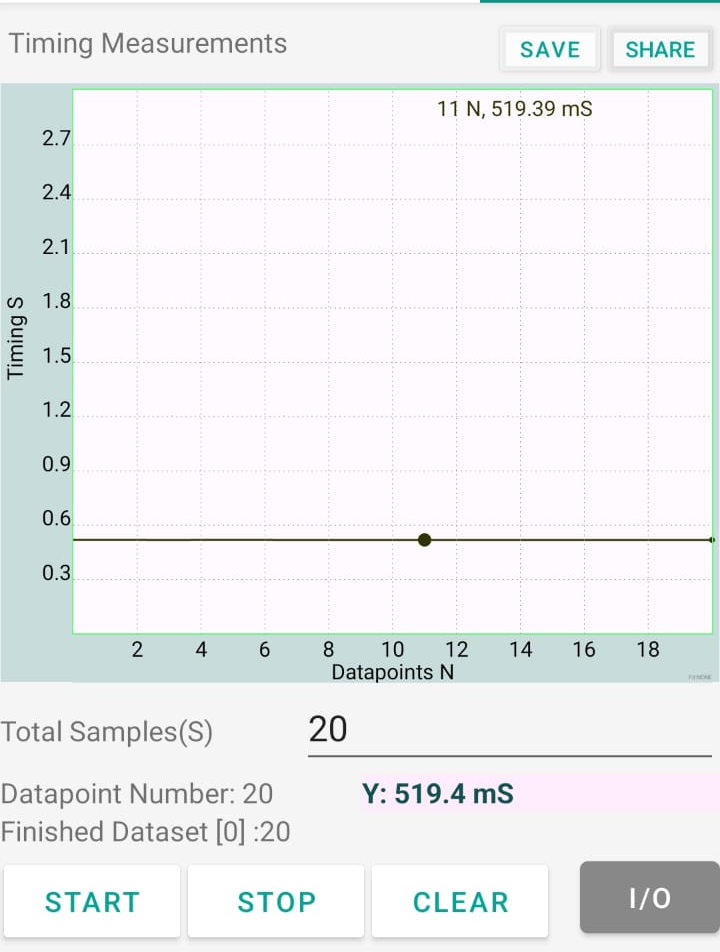
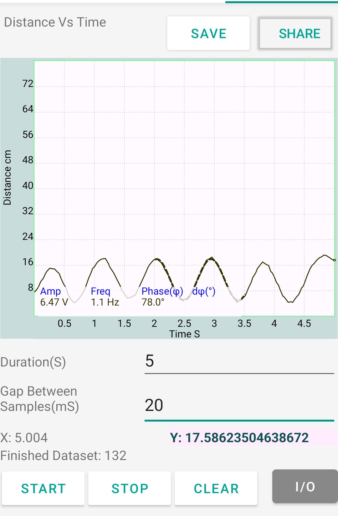
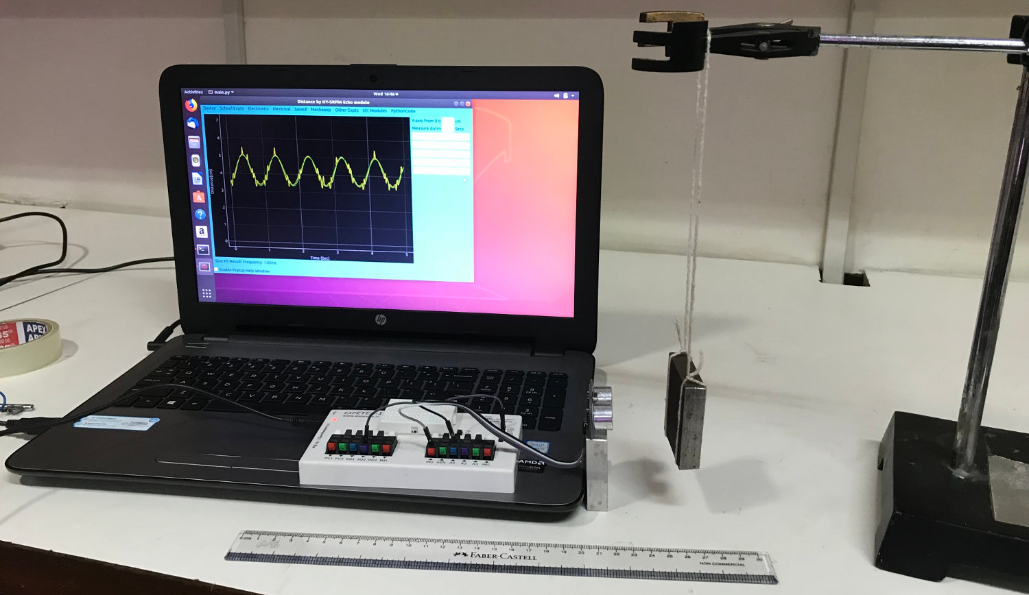
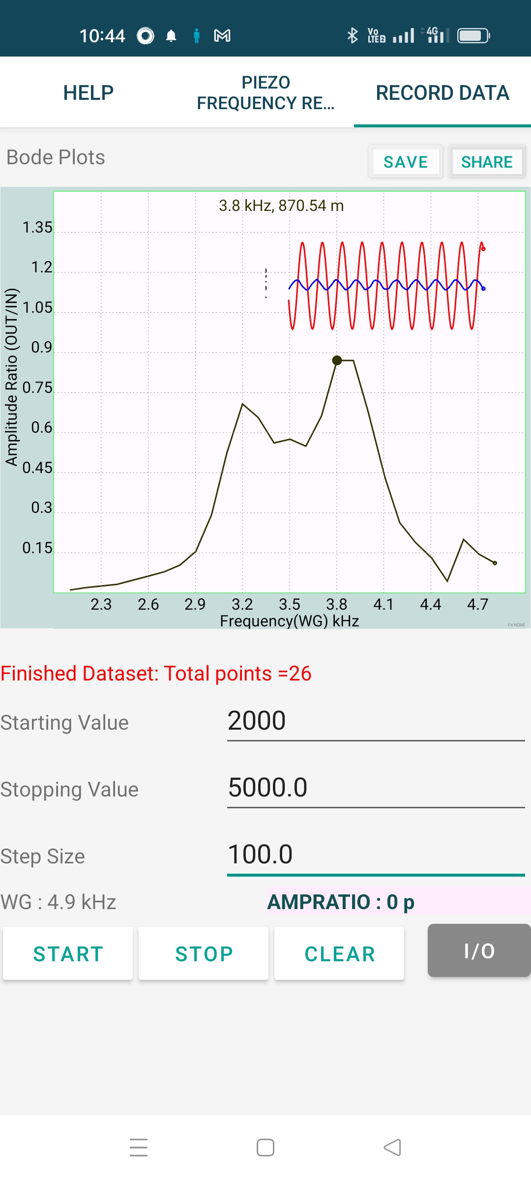
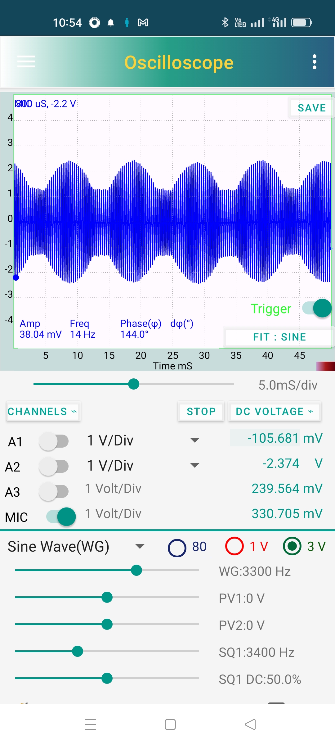
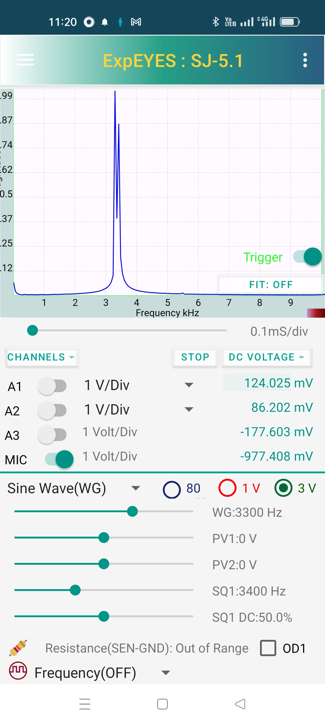
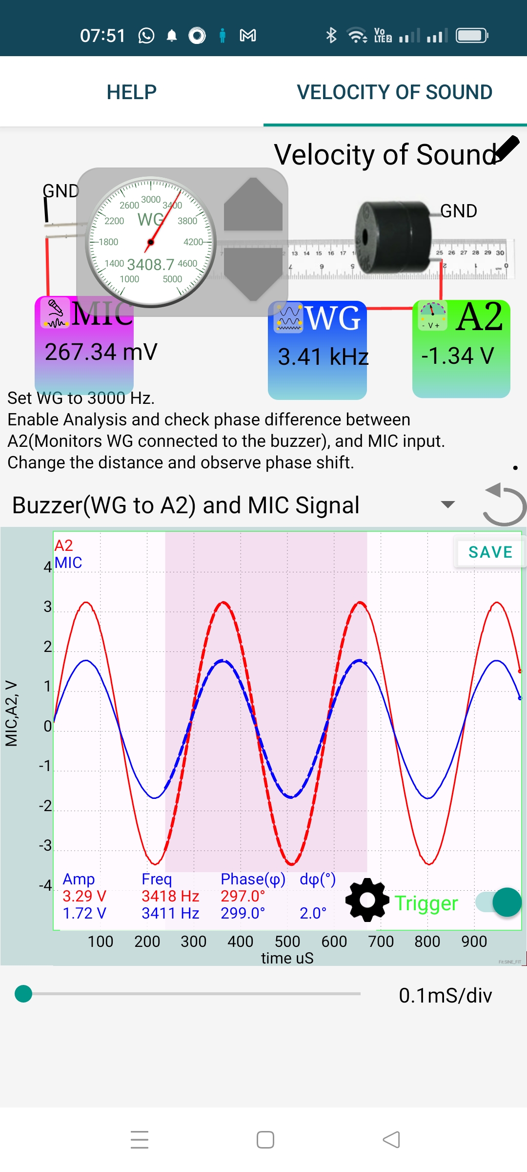
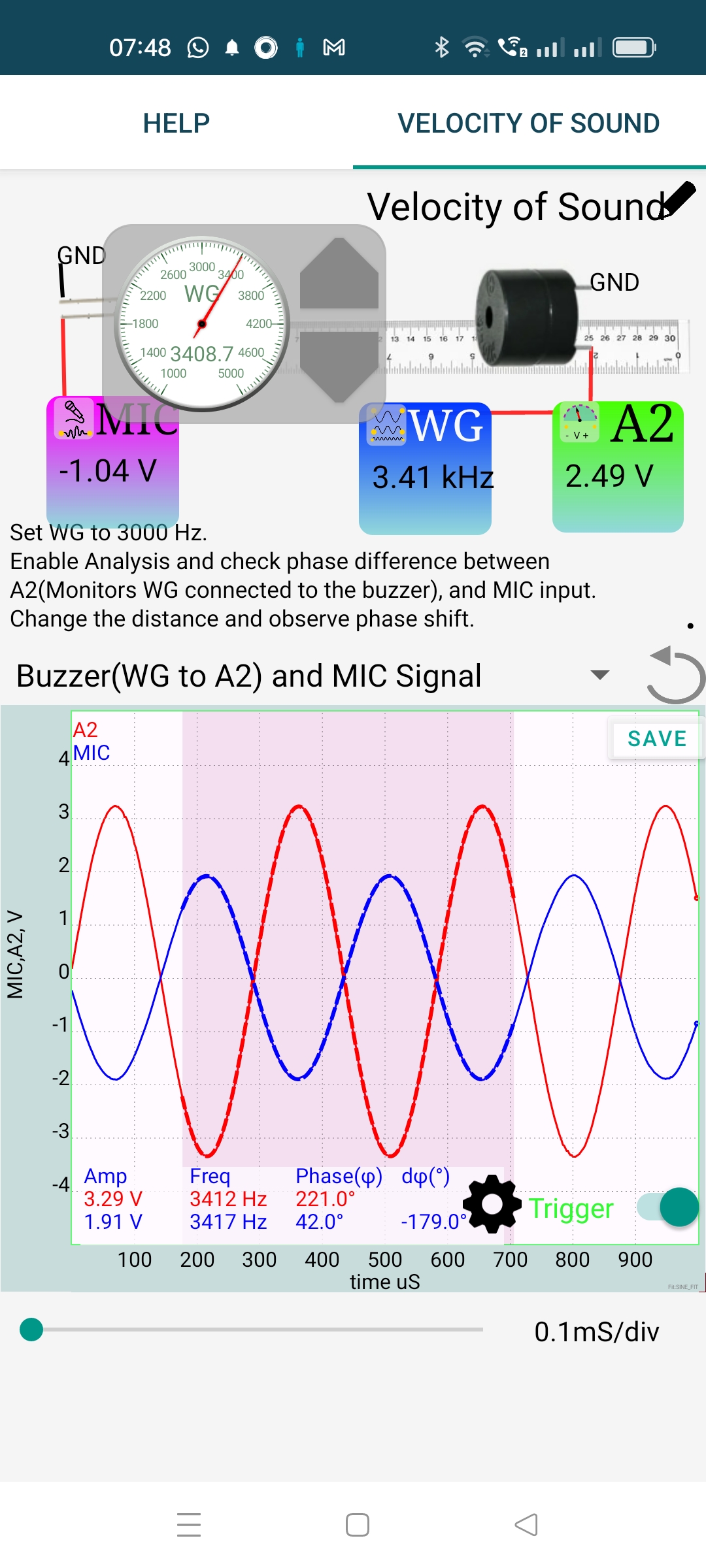
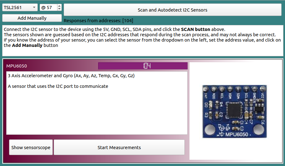
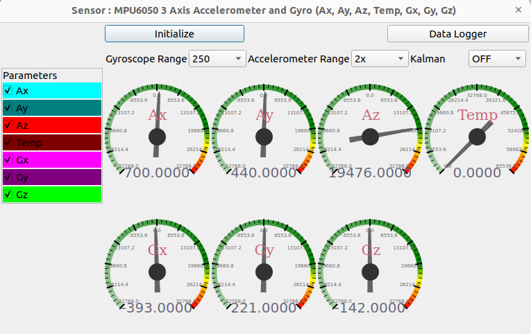
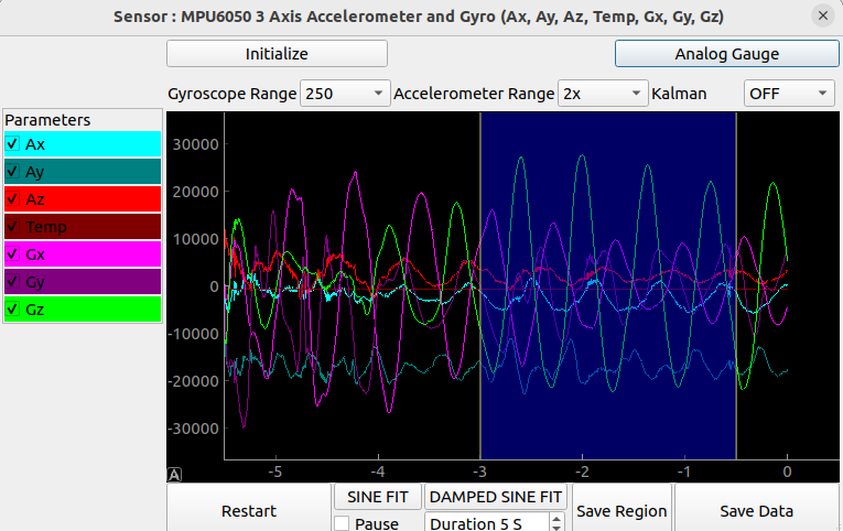
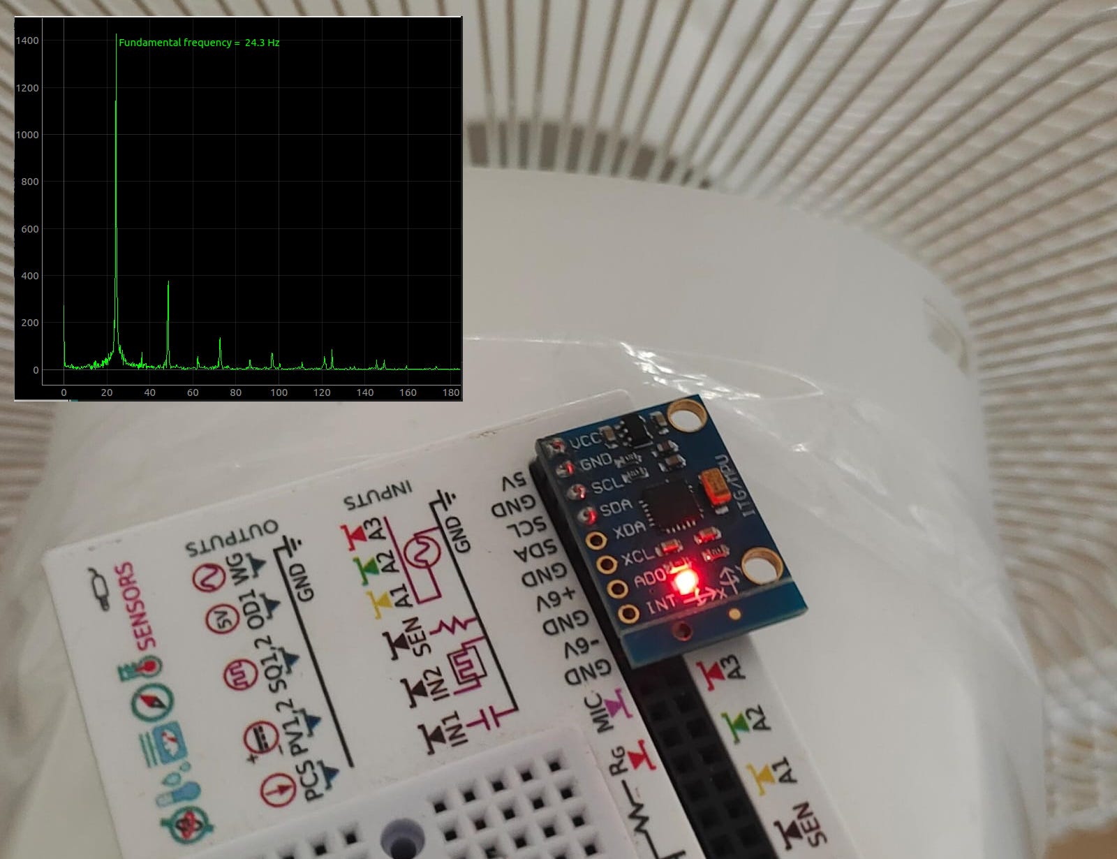
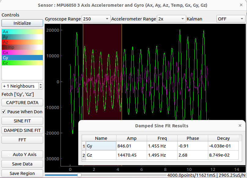
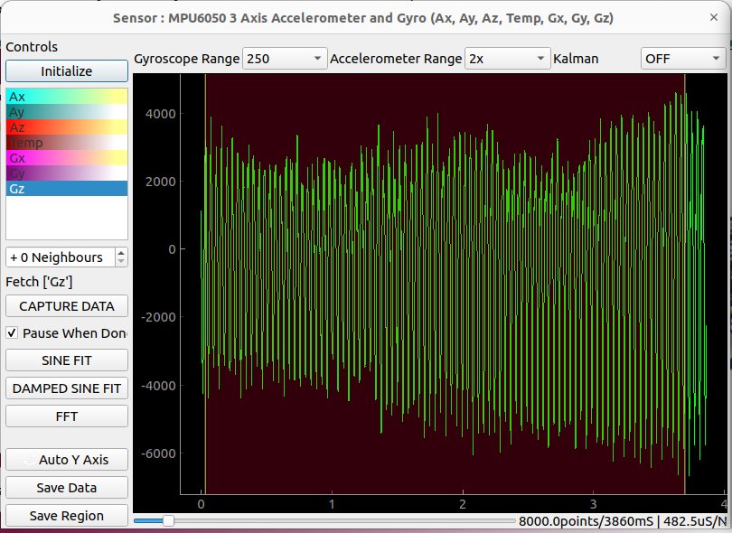
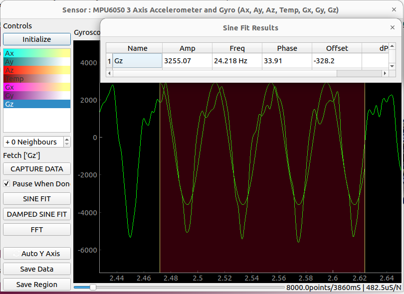
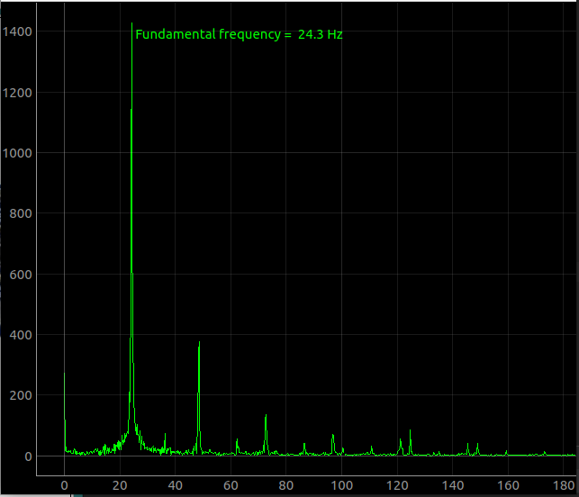

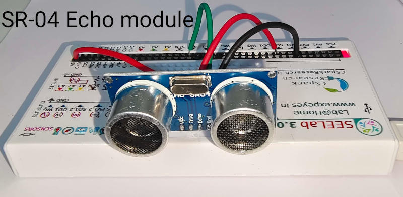
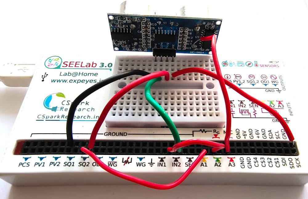
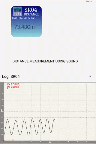
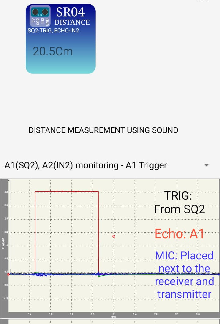 You can see a small ripple picked up by the microphone when the module transmits, and another smaller one when the echo is received. You can observe that these coincide
with the red graph(Echo) .
You can see a small ripple picked up by the microphone when the module transmits, and another smaller one when the echo is received. You can observe that these coincide
with the red graph(Echo) .