Experiment: V-I Characteristics of a Zener Diode
1. Aim
To plot the V-I characteristic of a Zener diode in both forward and reverse bias, and to measure the Zener breakdown voltage $V_Z$.
2. Apparatus / Components Required
- SEELab3 unit
- Zener diode: 3.3 V (e.g., 1N4728A or BZX55C3V3)
- Series resistor $R = 1\text{ k}\Omega$
- Connecting wires
- PC or Smartphone with SEELab3 software
3. Theory & Principle
The circuit and current measurement method are identical to the previous PN junction experiment — PV1 sweeps the applied voltage, A1 measures the voltage across the diode, and the current is:
\[I = \frac{V_{PV1} - V_{A1}}{R}\]What is new here is the reverse-bias behaviour.
A standard PN junction (like 1N4148) blocks almost completely in reverse bias. A Zener diode is specially doped so that at a precisely controlled reverse voltage — the Zener breakdown voltage $V_Z$ — the reverse current increases sharply while the voltage across the diode stays nearly constant. This is the property exploited in voltage regulators.
Two mechanisms produce breakdown:
- Zener effect (dominant for $V_Z \lesssim 5\text{ V}$): quantum mechanical tunnelling of electrons directly across the thin depletion region under a strong electric field.
- Avalanche effect (dominant for $V_Z \gtrsim 7\text{ V}$): carrier multiplication by impact ionisation.
Diodes in the 5–7 V range exhibit a mix of both. The 3.3 V Zener used here operates purely by the Zener (tunnelling) mechanism.
Why 3.3 V and not a higher-rated Zener?
PV1 on SEELab3 has a maximum output of $5\text{ V}$. To observe Zener breakdown in reverse bias, the reverse voltage across the diode must reach $V_Z$. With the diode reverse-biased:
\[V_{diode,\text{reverse}} = V_{A1} \approx -V_{PV1}\]So the reverse voltage available is limited to $\approx 5\text{ V}$. A 5.1 V or 6.2 V Zener would never reach breakdown — its characteristic would look identical to a plain reverse-biased diode. The 3.3 V Zener is ideal to drive into breakdown.
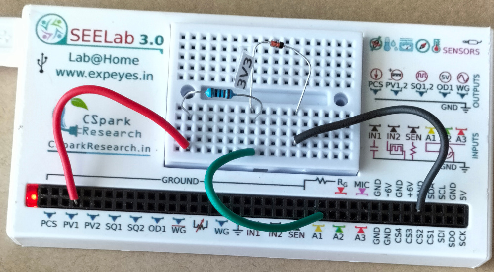
4. Circuit Diagram / Setup
Forward bias (same as PN junction experiment):
- Connect PV1 → $R$ → anode of Zener → GND (cathode).
- A1 at the anode (measures $V_D$ forward).
Reverse bias (to observe breakdown):
- No Change. PV1 can be varied from -5 to 5 Volts, so we can sweep from -5 to 0 volts to view the reverse bias characteristics
- Run both orientations back to back to get the complete two-quadrant characteristic.
5. Procedure
- Open the SEELab3 app and select the “Zener V-I” experiment.
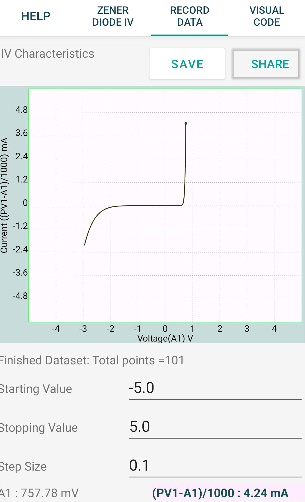
- Forward bias: Sweep PV1 from $0$ to $5\text{ V}$. The curve will look identical to the 1N4148 from the previous experiment — exponential rise beyond $\approx 0.6\text{ V}$.
- Reverse bias: No need to reverse the Zener on the breadboard because PV1 can output negative voltages as well. Sweep PV1 from $0$ to $-5\text{ V}$, watching A1. Beyond $V_Z$ the current starts increasing. Once PV1 is large enough to drive $V_{reverse} \geq V_Z$, the voltage at A1 clamps at $\approx 3.3\text{ V}$ while the current rises steeply.
- Use the record data tab to get the curve from -5V to 5V in a single two-quadrant V-I plot (reverse breakdown on the left, forward bias on the right).
6. Observation Table
| $R$: ____ $\Omega$ | Zener rated $V_Z$: ____ V |
6a. Reverse Bias — Breakdown Region
| $V_{PV1}$ (V) | $V_{A1}$ — reverse voltage (V) | $I = (V_{PV1} - V_{A1})/R$ (mA) |
|---|---|---|
| 0.5 | ||
| 1.0 | ||
| 1.5 | ||
| 2.0 | ||
| 2.5 | ||
| 2.8 | ||
| 3.0 | ||
| 3.3 |
6b. Summary
| Quantity | Value |
|---|---|
| Rated $V_Z$ (V) | 3.3 |
| Measured $V_Z$ — onset of breakdown (V) | |
| $V_Z$ at $I = 1\text{ mA}$ (V) | |
| $V_Z$ at $I = 2\text{ mA}$ (V) | |
| Change in $V_Z$ over $1$–$2\text{ mA}$ range (V) |
7. Results and Discussion
- In forward bias, the Zener exhibited the standard exponential V-I characteristic with $V_f \approx$ ____ V — identical to a normal silicon diode.
- In reverse bias, the current remained negligible until $V_{PV1}$ was sufficient to bring the reverse voltage to $\approx V_Z$.
- The measured breakdown voltage was ____ V, against the rated value of $3.3\text{ V}$ — a difference of ____ %, within the typical $\pm 5\%$ tolerance of Zener diodes.
- In the breakdown region, the voltage across the Zener changed by only ____ V as the current varied from $1\text{ mA}$ to $2\text{ mA}$, demonstrating the nearly constant-voltage (voltage-regulating) behaviour.
8. Precautions
- Series resistor is mandatory in both orientations: In the breakdown region, the Zener voltage is nearly constant — without $R$, the only thing limiting current is the source impedance of PV1, which is very small. The diode will be destroyed by excessive current. Always keep $R = 1\text{ k}\Omega$ in series.
- 3.3 V Zener only: Do not substitute a higher-voltage Zener (5.1 V, 6.2 V, etc.) — PV1 cannot supply enough voltage to drive it into breakdown and the reverse characteristic will appear flat and featureless.
- Check diode orientation carefully when switching between forward and reverse bias — it is easy to re-insert the Zener in the same orientation by mistake.
9. Troubleshooting
| Symptom | Possible Cause | Corrective Action |
|---|---|---|
| Reverse characteristic is flat — no breakdown visible | Zener $V_Z > 3.3\text{ V}$, or diode is a similar looking regular diode like IN4148. | Confirm a 3.3 V Zener is used |
| $V_{A1}$ clamps well below 3.3 V | Zener is a lower-rated part than labelled, or a plain PN junction accidentally used. | Check part marking; test with multimeter in diode mode. |
| Very high current immediately in reverse bias | $R$ missing or shorted; Zener already damaged. | Check $R$ connection; replace Zener if shorted in both directions. |
10. Viva-Voce Questions
Q1. What distinguishes a Zener diode from an ordinary PN junction diode?
Ans: Both are PN junctions, but a Zener is heavily doped on both sides, creating a very narrow, intense depletion region. This produces a precisely controlled and sharp reverse breakdown voltage $V_Z$, after which large reverse current flows at nearly constant voltage. An ordinary diode (like 1N4148) also breaks down in reverse, but at a higher and less controlled voltage — and it is not designed to survive sustained breakdown current. A Zener is designed to operate continuously in breakdown as a voltage reference or regulator.
Q2. What is the Zener effect, and why does it dominate in low-voltage ($< 5\text{ V}$) Zeners?
Ans: The Zener effect is quantum mechanical tunnelling — valence electrons tunnel directly through the thin depletion region potential barrier without needing enough thermal energy to surmount it classically. It dominates when the depletion region is very narrow (achieved by heavy doping), because the tunnelling probability falls exponentially with barrier width. Low-$V_Z$ Zeners are very heavily doped, giving extremely thin depletion regions where tunnelling is significant. Higher-voltage Zeners have wider depletion regions where tunnelling is negligible and avalanche multiplication takes over instead.
Q4. How would a Zener diode be used as a simple voltage regulator?
Ans: Connect the Zener in reverse bias with a series resistor $R_s$ between the unregulated supply $V_{in}$ and the Zener cathode (anode to GND). The load is connected in parallel with the Zener. As long as $V_{in} > V_Z$ and the current through $R_s$ is sufficient to keep the Zener in breakdown, the output voltage is held at $V_Z$ regardless of load current variations. $R_s$ must be chosen so the Zener stays in breakdown under maximum load and doesn't exceed its power rating $P_Z = V_Z \cdot I_{Z,max}$ under minimum load.
Q5. Why does a 3.3 V Zener have a negative temperature coefficient while a 6.2 V Zener has a positive one?
Ans: The Zener effect (tunnelling, $< 5\text{ V}$) has a negative temperature coefficient — higher temperature increases the lattice vibrations, which slightly widens the effective barrier and reduces tunnelling, lowering the breakdown voltage. The avalanche effect ($> 7\text{ V}$) has a positive temperature coefficient — higher temperature reduces carrier mean free path (more scattering), making it harder to accelerate carriers to ionisation energy, so a higher voltage is needed for breakdown. Diodes near $5$–$6\text{ V}$ have near-zero temperature coefficient because the two effects partially cancel — the $6.2\text{ V}$ Zener is commonly used as a precision temperature-stable voltage reference for this reason.