Experiment: Single Transistor Amplifier
1. Aim
To build and test a single-stage common-emitter transistor amplifier, measure its input/output waveforms, and observe how bias point and input amplitude affect gain and distortion.
2. Apparatus / Components Required
- SEELab3 unit
- NPN transistor (recommended: 2N2222)
- Bias resistor: 100 kOhm (base bias from PV2)
- Signal divider resistors: 1 kOhm and 2.2 kOhm (to attenuate WG signal)
- Coupling capacitor for base input (AC coupling)
- Collector and emitter resistors as per your standard amplifier setup
- Breadboard and connecting wires
- PC / mobile running SEELab3 interface

Mobile App
Desktop App
3. Theory & Principle
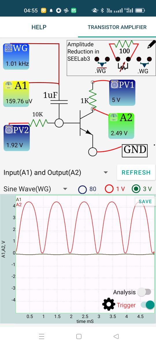
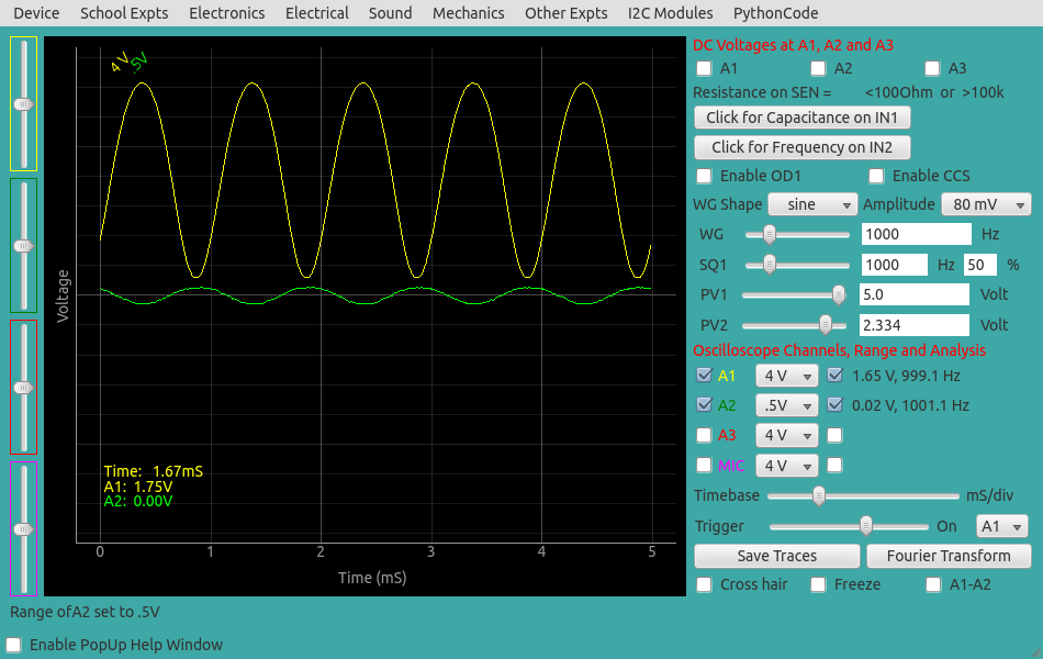
This experiment uses a common-emitter (CE) transistor amplifier. The input AC signal is applied to the base through a coupling capacitor so that the DC bias condition is not disturbed.
Because CE gain can be high, a small input signal is needed to avoid clipping. The ExpEYES method uses a 1 kOhm : 2.2 kOhm divider to reduce the waveform-generator signal to around a few tens of millivolts at the base input.
The transistor operating point (Q-point) is set by base bias through a 100 kOhm resistor, controlled by PV2:
- If bias is too low -> cut-off during part of the cycle (bottom clipping).
- If bias is too high -> saturation during part of the cycle (top clipping).
- At proper bias -> maximum undistorted output swing.
Why small input is important
For linear amplification, the transistor must stay in active region over the signal cycle. If input amplitude is too high, the instantaneous operating point enters cut-off/saturation, causing waveform distortion.
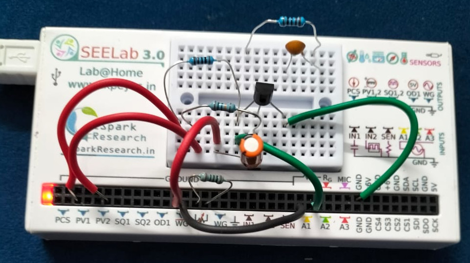
4. Circuit Diagram / Setup
- Build the CE amplifier wiring as in the output-characteristics style circuit (collector resistor, emitter to ground path, base bias through 100 kOhm).
- Connect WG output to a divider network using 1 kOhm and 2.2 kOhm.
- Feed the attenuated signal to the transistor base through a coupling capacitor.
- Monitor:
- A2 -> input signal at base side (after divider/coupling).
- A1 -> output signal at collector.
- Use PV2 to adjust base bias for minimum distortion.
SEELab3 note
SEELab3 allows reducing WGbar amplitude using an external gain resistor. A 100 Ohm resistor can reduce approximately 3 V to around 30 mV, suitable for low-distortion transistor amplification.
5. Procedure
- Power the setup and open the relevant transistor amplifier tool/scope view in SEELab3.
- Start with a low-frequency sine input (for example, 500 Hz to 1 kHz).
- Keep input amplitude small using the divider (or WGbar attenuation method).
- Observe input on A2 and output on A1.
- Slowly vary PV2:
- find a bias point where output is centered and least distorted.
- Increase input amplitude gradually and note onset of clipping.
- Record waveforms and estimate voltage gain:
- Try these improvements and compare:
- lower input amplitude,
- higher collector supply (if external safe supply is used),
- lower-gain transistor.
6. Observation Table
| Trial | $V_{in,pp}$ (mV) | $V_{out,pp}$ (V) | Bias setting (PV2) | Gain $A_v$ | Distortion observed |
|---|---|---|---|---|---|
| 1 | |||||
| 2 | |||||
| 3 | |||||
| 4 |
7. Results and Discussion
- The CE stage produced an amplified output with phase inversion (approximately 180 degrees) relative to input.
- Best amplification occurred at an intermediate base bias where clipping was minimal.
- At low bias the output showed cut-off clipping; at high bias it showed saturation clipping.
- Measured voltage gain was $A_v =$ ____ under near-linear conditions.
8. Precautions
- Keep input small; CE stages distort quickly for large base drive.
- Always use coupling capacitor at base input to prevent bias shift by WG DC component.
- Verify transistor pinout before powering the circuit.
- Do not exceed safe collector current or device power limits.
- Ensure common ground between SEELab3 and the circuit.
9. Troubleshooting
| Symptom | Possible Cause | Corrective Action |
|---|---|---|
| No output on A1 | Wrong transistor pinout / open collector path | Recheck E-B-C pin connections and resistor wiring |
| Output heavily clipped even at low input | Bias point too low/high | Adjust PV2 for centered undistorted waveform |
| Input appears too large | Divider not connected correctly | Verify 1 kOhm and 2.2 kOhm divider wiring |
| DC shift at base input | Missing/incorrect coupling capacitor | Replace/add base coupling capacitor |
| Very low gain | Transistor damaged or wrong resistor values | Check component values and swap transistor |
10. Viva-Voce Questions
Q1. Why is a coupling capacitor used at the transistor base?
Ans: The capacitor passes AC signal and blocks DC. This allows the signal to be superimposed on the chosen DC bias point without disturbing the base bias network.
Q2. Why does distortion occur if bias is not set correctly?
Ans: If the Q-point is too near cut-off or saturation, part of the input cycle drives the transistor out of active region. The output then clips, producing nonlinear distortion.
Q3. Why is input attenuated before feeding the base?
Ans: CE voltage gain can be high. A large input overdrives the transistor, so attenuating input to tens of millivolts keeps operation in the linear region.
Q4. What is the phase relation between input and output in CE amplifier?
Ans: The output at collector is inverted with respect to input by about 180 degrees.
Q5. Name three ways to reduce distortion in this experiment.
Ans: Reduce input amplitude, choose a better bias point (PV2 adjustment), and use a higher collector supply (within safe limits) or a transistor with lower gain.