Experiment: Output Characteristics of a PNP Transistor
1. Aim
To plot the output characteristics ($I_C$ vs $V_{CE}$) of a PNP transistor (2N3906) in common-emitter configuration for a family of base currents.
2. Apparatus / Components Required
- SEELab3 unit (utilizing PV1 and PV2)
- PNP transistor: 2N3906
- Collector resistor $R_C = 1\text{ k}\Omega$
- Base resistor $R_B = 100\text{ k}\Omega$
- Connecting wires
- PC or Smartphone with SEELab3 software
3. Theory & Principle
The PNP transistor is the “dual” of the NPN. While the operational logic is the same, the polarities of all voltages and the directions of all currents are reversed. In a PNP transistor, holes are the majority carriers injected from the Emitter into the Base.
Key Differences for PNP:
- $V_{BE}$: Must be negative (Base lower than Emitter) to forward-bias the junction ($\approx -0.6\text{ V}$).
- $V_{CE}$: Operated in the negative range for the active region.
- Currents: $I_B$ and $I_C$ flow out of the base and collector terminals respectively.
SEELab3 Implementation (Negative Range)
Since SEELab3 can output negative voltages ($-5\text{V}$ to $+5\text{V}$ on PV1, and $-3\text{V}$ to $+3\text{V}$ on PV2), we can bias the PNP transistor conventionally by using the negative supply range:
- Emitter: Connected to GND ($0\text{V}$).
- Collector: Connected to PV1 via 1K (swept from $0\text{V}$ to $-5\text{V}$).
- Base: Connected to PV2 via 100K (set to negative values to forward-bias the Emitter-Base junction).
The current calculations : \(I_C = \frac{V_{PV1} - V_{A1}}{R_C} \qquad I_B = \frac{V_{PV2} - V_{A2}}{R_B}\)
4. Circuit Diagram / Setup
- Emitter: Connect directly to GND.
- Collector: Connect to PV1 through the $1\text{ k}\Omega$ resistor ($R_C$). Connect A1 to the Collector to monitor $V_C$.
- Base: Connect to PV2 through the $100\text{ k}\Omega$ resistor ($R_B$). Connect A2 to the Base to monitor $V_B$.
5. Procedure
- Open the SEELab3 app and select the “PNP Output Characteristics” experiment.
- Base Bias: Set PV2 to a small negative voltage (e.g., $-1.0\text{V}$ to $-2.0\text{V}$). This ensures $V_{BE} \approx -0.6\text{V}$ and establishes a constant $I_B$.
- Collector Sweep: The software will sweep PV1 from $0\text{V}$ down to $-5\text{V}$.
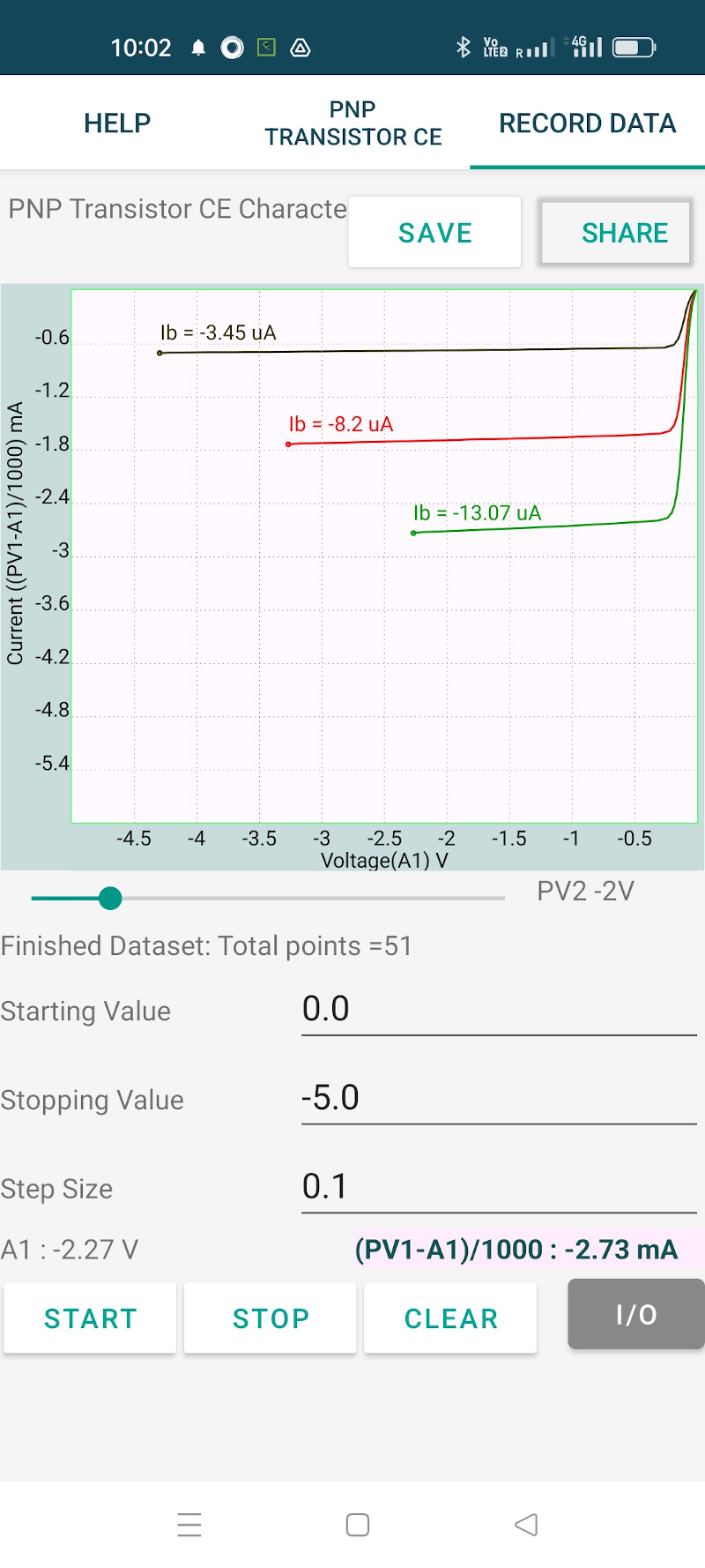
- Observe: Note the $I_C$ vs $V_{CE}$ curve. It should appear in the third quadrant of the graph (negative $X$ and negative $Y$ axes).
- Repeat for different values of PV2 to generate a family of curves.
- Calculate the current gain $h_{FE} = I_C / I_B$ in the linear (active) region.
Mobile App (Negative Quadrant)
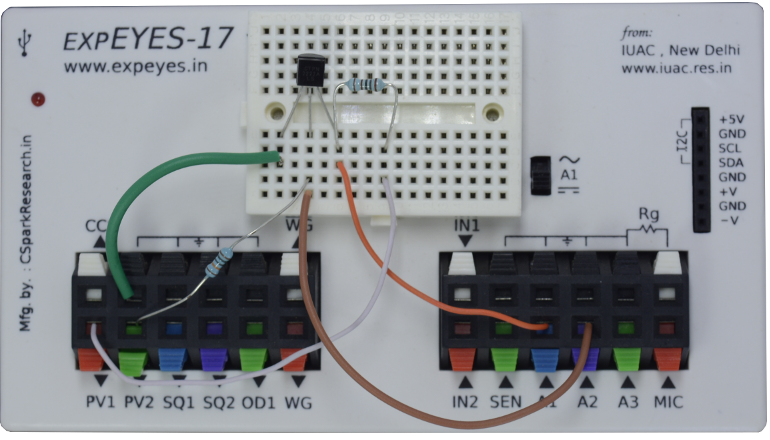
Hardware Setup
6. Observation Table
| Transistor: 2N3906 | $R_C$: $1\text{ k}\Omega$ | $R_B$: $100\text{ k}\Omega$ |
| $V_{PV2}$ (V) | $I_B$ ($\mu$A) | $I_C$ (at $V_{CE} = -3\text{V}$) | $h_{FE} = I_C / I_B$ |
|---|---|---|---|
| -1.2 | |||
| -1.5 | |||
| -2.0 | |||
| -2.5 |
7. Results and Discussion
- The PNP output characteristics were successfully plotted in the negative voltage/current region.
- The curves show a distinct Saturation region (near $0\text{V}$) and an Active region (plateau).
- The average current gain ($h_{FE}$) was found to be ____.
8. Precautions
- Polarity Check: Ensure you are using the negative range of PV1 and PV2. Applying large positive voltages to a PNP base-emitter junction in this configuration can damage the device.
- Pinout: Double-check the 2N3906 pins (E-B-C). It is often identical to the 2N2222, but reversed orientation is a common source of flat-line results.
- Heat: Inductors or transistors can get warm if $I_C$ is too high; keep $I_C$ within the recommended $10\text{ mA}$ limit for educational plotting.
9. Troubleshooting
| Symptom | Possible Cause | Corrective Action |
|---|---|---|
| Flat line at $I_C = 0$ | Base is not forward biased. | Ensure PV2 is negative enough (at least $-0.8\text{V}$ to $-1\text{V}$). |
| A1 reads $0\text{V}$ always | Open collector circuit. | Check $R_C$ and collector jumper wire. |
| Curves go upward (Positive) | NPN used by mistake. | Check the transistor part number; NPN and PNP look identical. |
10. Viva-Voce Questions
Q1. Why are the characteristics of a PNP transistor plotted in the third quadrant?
Ans: In a PNP transistor, the collector is biased negatively with respect to the emitter ($V_{CE} < 0$) and the collector current flows out of the terminal ($I_C < 0$). In a Cartesian coordinate system, negative X and negative Y represent the third quadrant.
Q2. What are the majority charge carriers in a PNP transistor?
Ans: Holes. They are injected from the p-type emitter into the n-type base.
Q3. What happens if you connect the PNP emitter to a positive supply and the collector to GND?
Ans: This is an alternative way to bias a PNP. In that case, all measurements would be positive relative to GND, but $V_{CE}$ (Emitter to Collector) would still be a negative value. SEELab3's ability to output negative PV1/PV2 allows us to keep the Emitter at GND for simpler conceptual mapping.
Q4. How does the mobility of holes in PNP compare to electrons in NPN?
Ans: Hole mobility is generally lower than electron mobility. Consequently, PNP transistors are typically slower and have lower frequency response than equivalent NPN transistors.
Q5. Define the 'Early Effect' seen in output characteristics.
Ans: It is the slight upward slope of the $I_C$ curves in the active region. As $\lvert V_{CE} \rvert$ increases, the collector-base depletion region widens, effectively narrowing the base width and slightly increasing the current gain.