Experiment: Output Characteristics of an NPN Transistor (Common-Emitter)
1. Aim
To plot the output characteristics ($I_C$ vs $V_{CE}$ for fixed $I_B$) and the transfer characteristics ($I_C$ vs $I_B$) of an NPN transistor in the common-emitter configuration, and to determine the current gain $h_{FE}$ and output impedance from the curves.
2. Apparatus / Components Required
- SEELab3 unit (both PV1 and PV2 required)
- NPN transistor: 2N2222 ($h_{FE} \approx 200$)
- Collector resistor $R_C = 1\text{ k}\Omega$
- Base resistor $R_B = 100\text{ k}\Omega$
- Connecting wires
- PC with Python 3 (libraries:
expeyes,numpy,scipy,matplotlib)
3. Theory & Principle

In the common-emitter (CE) configuration, the emitter is the common terminal between input (base) and output (collector) circuits. The transistor has three operating regions:
- Cut-off: $V_{BE} < 0.6\text{ V}$ — both junctions reverse biased; $I_C \approx 0$.
- Active: $V_{BE} \approx 0.7\text{ V}$, $V_{CE} > V_{CE,sat}$ — base-emitter forward biased, base-collector reverse biased. Collector current is controlled by base current: $I_C = h_{FE} \cdot I_B$.
- Saturation: $V_{CE} < V_{CE,sat} \approx 0.2\text{ V}$ — both junctions forward biased; $I_C$ no longer controlled by $I_B$.
The DC current gain:
\[h_{FE} = \frac{I_C}{I_B} \bigg|_{\text{active region}}\]For the 2N2222, $h_{FE} \approx 200$, meaning a base current of $10\text{ }\mu\text{A}$ drives a collector current of $\approx 2\text{ mA}$.
Indirect current measurement
Both $I_B$ and $I_C$ are measured without ammeters, using the same technique as the diode experiments:
\[I_B = \frac{V_{PV2} - V_{A2}}{R_B} \qquad I_C = \frac{V_{PV1} - V_{A1}}{R_C}\]where A2 monitors the base voltage and A1 monitors the collector voltage.
Output impedance
In the active region the $I_C$ vs $V_{CE}$ curves are nearly — but not perfectly — horizontal. The slight upward slope gives the output impedance:
\[r_o = \frac{\Delta V_{CE}}{\Delta I_C}\bigg|_{I_B = \text{const}}\]A steep slope means low $r_o$ (less ideal current source); a flat curve means high $r_o$ (more ideal).
4. Circuit Diagram / Setup
- Connect PV2 → $R_B$ ($100\text{ k}\Omega$) → Base of 2N2222. Connect A2 at the Base.
- Connect PV1 → $R_C$ ($1\text{ k}\Omega$) → Collector. Connect A1 at the Collector.
- Connect Emitter to GND.
5. Procedure
Part A — Output characteristics (app-based)
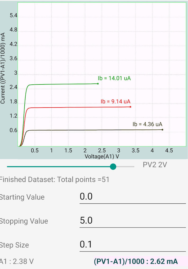
- Open the SEELab3 app and select the “NPN Output Characteristics” experiment.
- Set PV2 to a fixed value (e.g., $1.5\text{ V}$) to establish a base current $I_B \approx (1.5 - 0.7)/100\text{k} = 8\text{ }\mu\text{A}$.
- The software sweeps PV1 from $0$ to $3.3\text{ V}$ in steps, recording $V_{A1}$ (collector voltage) at each step and computing $I_C = (V_{PV1} - V_{A1})/R_C$.
- The $I_C$ vs $V_{CE}$ curve is plotted. Identify the saturation region (steep rise, $V_{CE} < 0.3\text{ V}$) and the active region (flat plateau).
- Repeat for at least three different PV2 values to generate a family of curves.
Part B — Transfer characteristics and $h_{FE}$
- Fix $V_{PV1}$ at a value that keeps the transistor in the active region (e.g., $2\text{ V}$).
- Sweep PV2 in steps, recording $I_B$ and the corresponding $I_C$ at each step.
- Plot $I_C$ vs $I_B$ — the slope of this line is $h_{FE}$.
Part C — Python automation
The following Python programs automate the sweep and analysis. Download them from the links below:
- npn-ce-output.py — sweeps PV1 for each of several PV2 (base current) values and saves $V_{CE}$, $I_C$, $I_B$ to a CSV file.
- Sample data (npn-ce-output.csv) — reference dataset for testing the analysis script.
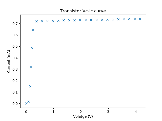
- npn-ce-output-analyse.py — reads the CSV, plots the family of $I_C$ vs $V_{CE}$ curves, and prints $h_{FE}$ and $r_o$ for each base current.
- npn-ce-ibic.py — plots the transfer characteristic ($I_B$ vs $I_C$).
- npn-ce-ibic-lsfit.py — fits the $I_B$ vs $I_C$ data by least squares to extract $h_{FE}$.
Mobile App
Python Output
6. Observation Table
| Transistor: ____ | $R_C$: ____ $\Omega$ | $R_B$: ____ $\Omega$ |
6a. Output Characteristics — $I_C$ vs $V_{CE}$
For each $I_B$ row, record $I_C$ (mA) at the listed $V_{CE}$ values.
| $I_B$ ($\mu$A) | $I_C$ at $V_{CE}=0.2$ V | $I_C$ at $0.5$ V | $I_C$ at $1.0$ V | $I_C$ at $1.5$ V | $I_C$ at $2.0$ V | $I_C$ at $2.5$ V |
|---|---|---|---|---|---|---|
| ~7 | ||||||
| ~9 | ||||||
| ~11 | ||||||
| ~13 |
6b. Transfer Characteristics and $h_{FE}$
| $I_B$ ($\mu$A) | $I_C$ (mA) | $h_{FE} = I_C / I_B$ |
|---|---|---|
| Mean $h_{FE}$ |
6c. Output Impedance (active region, from Python slope)
| $I_B$ ($\mu$A) | Slope $\Delta I_C / \Delta V_{CE}$ (mA/V) | $r_o = 1/\text{slope}$ (k$\Omega$) |
|---|---|---|
7. Results and Discussion
- The output characteristics showed a clear saturation region ($V_{CE} < \approx 0.3\text{ V}$) where $I_C$ rises steeply, and an active region ($V_{CE} > 0.5\text{ V}$) where $I_C$ is nearly constant and proportional to $I_B$.
- The measured current gain was $h_{FE} =$ ____, against the datasheet value of $\approx 200$ for the 2N2222.
- The output impedance in the active region was $r_o \approx$ ____ k$\Omega$, indicating that the transistor acts as a good (though not ideal) current source in CE configuration.
- Increasing $I_B$ shifted the active-region plateau upward by $h_{FE} \times \Delta I_B$, confirming the linear relationship between base and collector currents.
8. Precautions
- Never leave the base floating: A floating base picks up stray voltages and drives the transistor into an unpredictable state. Always connect $R_B$ from PV2 to the base, even when PV2 = 0 V.
- PV1 limit is 3.3 V: The collector sweep is limited to $V_{CE,max} \approx 3.3\text{ V}$. This is sufficient to clearly observe both the saturation knee and the active plateau for the base currents used.
- Power dissipation: At $I_C = 2\text{ mA}$ and $V_{CE} = 3\text{ V}$, the transistor dissipates $P = 6\text{ mW}$ — well within the 2N2222’s $625\text{ mW}$ limit. Do not use base currents that push $I_C$ beyond $3\text{ mA}$ with this setup.
- Transistor pinout: The 2N2222 in TO-18 metal can and TO-92 plastic package have different pin orders. Verify the pinout (E, B, C) from the datasheet before inserting.
9. Troubleshooting
| Symptom | Possible Cause | Corrective Action |
|---|---|---|
| $I_C$ is zero for all $V_{CE}$ | Base not connected or PV2 too low to forward-bias $V_{BE}$. | Ensure PV2 $\geq 1.3\text{ V}$ (so $V_{BE} \geq 0.6\text{ V}$); check $R_B$ connection. |
| $I_C$ saturates immediately — curves don’t separate | Transistor pinout wrong (C and E swapped). | Re-check pinout from datasheet; swap collector and emitter connections. |
| All curves overlap — no $I_B$ dependence visible | A2 not connected to base; $I_B$ not actually changing with PV2. | Verify A2 is at the base node, not at PV2 directly. |
| $h_{FE}$ far below 200 | Wrong transistor, or transistor damaged by previous overcurrent. | Replace 2N2222; verify with multimeter in $h_{FE}$ mode if available. |
10. Viva-Voce Questions
Q1. Why is the common-emitter configuration the most widely used of the three BJT configurations?
Ans: The CE configuration provides both current gain ($h_{FE} \gg 1$) and voltage gain simultaneously, giving the highest power gain of the three configurations (CB, CE, CC). The input impedance is moderate (a few k$\Omega$) and the output impedance is high (tens to hundreds of k$\Omega$) — a useful combination for amplifier stages. The CB configuration offers no current gain; the CC (emitter follower) offers no voltage gain. For most amplification applications, CE is therefore the natural choice.
Q2. What happens at the transistor's operating point as $V_{CE}$ falls below $V_{CE,sat} \approx 0.2\text{ V}$?
Ans: When $V_{CE} < V_{CE,sat}$, the base-collector junction also becomes forward biased (in addition to the base-emitter junction). The transistor enters saturation: both junctions are conducting, the collector can no longer absorb all the minority carriers injected from the base, and $I_C$ is no longer controlled by $I_B$. Instead $I_C$ is limited by the external circuit ($V_{CE}/R_C$). The transistor acts like a closed switch in saturation — useful in digital logic, but not for linear amplification.
Q3. The active-region $I_C$ vs $V_{CE}$ curves slope slightly upward rather than being perfectly flat. What causes this?
Ans: This is the Early effect (base-width modulation). As $V_{CE}$ increases, the reverse bias on the base-collector junction increases, widening the depletion region and narrowing the effective base width. A narrower base means less recombination of minority carriers in transit, so more reach the collector — $I_C$ increases slightly with $V_{CE}$ even at constant $I_B$. Extrapolating the active-region curves backward, they all converge at a negative voltage on the $V_{CE}$ axis called the Early voltage $V_A$ (typically 50–200 V for BJTs), which characterises the output impedance: $r_o = V_A / I_C$.
Q4. How are both $I_B$ and $I_C$ measured without ammeters in this experiment?
Ans: By measuring the voltage drop across the known series resistors $R_B$ and $R_C$ and applying Ohm's law. $I_B = (V_{PV2} - V_{A2})/R_B$ — the numerator is the voltage across $R_B$ (PV2 sets one end, A2 measures the base). $I_C = (V_{PV1} - V_{A1})/R_C$ — the numerator is the voltage across $R_C$ (PV1 sets one end, A1 measures the collector). Since all four voltages are known from the SEELab3 channels and the resistors are known, both currents are fully determined. This indirect technique was introduced in the diode V-I experiment.
Q5. Why does $h_{FE}$ vary with collector current, and what does this mean for amplifier design?
Ans: $h_{FE}$ is not truly constant — it peaks at moderate $I_C$ (typically a few milliamps for a small-signal transistor) and falls at both very low currents (where recombination in the base dominates) and very high currents (where high-level injection effects reduce efficiency). This means an amplifier's gain changes with signal level, introducing nonlinearity (harmonic distortion). In practice, amplifiers are biased at the $I_C$ where $h_{FE}$ is most stable and feedback is used to stabilise gain against $h_{FE}$ variations. The transfer characteristic ($I_C$ vs $I_B$) measured in Part B directly reveals this non-constancy.