Experiment: Half-Wave Rectifier Using a PN Junction Diode
1. Aim
To study the rectifying action of a PN junction diode by constructing a half-wave rectifier, to observe the difference between the ideal textbook waveform and the actual output, to investigate the effect of junction capacitance on the reverse-half output, and to study the smoothing effect of a filter capacitor on the rectified waveform.
2. Apparatus / Components Required
- SEELab3 or ExpEYES-17 unit
- PN junction diode — 1N4148 (low junction capacitance, $C_j \approx 4\text{ pF}$)
- PN junction diode — 1N4007 (higher junction capacitance, $C_j \approx 20\text{ pF}$) for comparison
- Load resistor $R_L = 1\text{ k}\Omega$
- Filter capacitor $C = 1\text{ }\mu F$
- Breadboard and connecting wires
- PC or Smartphone with SEELab3 / ExpEYES software
3. Theory & Principle
3.1 The PN Junction as a Rectifier
A PN junction diode conducts current freely when forward biased (anode positive with respect to cathode) and blocks current when reverse biased. When an AC sinusoidal voltage is applied to a series circuit of a diode and a load resistor $R_L$:
- Positive half-cycle: The diode is forward biased and conducts. Current flows through $R_L$ and a positive output voltage appears.
- Negative half-cycle: The diode is reverse biased and ideally blocks all current. The output voltage across $R_L$ is zero.
Since only one half of the AC cycle appears at the output, this is called half-wave rectification.
3.2 Deviation from the Ideal Textbook Waveform
Many textbooks depict the output as a perfect half-sinusoid that begins exactly at $0\text{ V}$ and reaches the same peak as the input. The actual output differs in two important ways:
Forward voltage drop ($V_f$): A real silicon diode requires a minimum forward voltage of approximately $0.6$–$0.7\text{ V}$ before it begins to conduct significantly. The output therefore:
- Starts conducting only when $V_{in} > V_f \approx 0.6\text{ V}$ (the threshold or cut-in voltage)
- Has a peak amplitude reduced by $V_f$ compared to the input peak:
For $V_{in,\text{peak}} = 3\text{ V}$ and $V_f \approx 0.6\text{ V}$, the output peak is approximately $2.4\text{ V}$.
3.3 Junction Capacitance and Reverse-Half Leakage
Every PN junction has a small junction capacitance $C_j$ in parallel with the ideal diode. Its value depends on the diode type:
| Diode | $C_j$ (typical) | Application |
|---|---|---|
| 1N4148 | $\approx 4\text{ pF}$ | Signal / high-speed switching |
| 1N4007 | $\approx 20\text{ pF}$ | Mains rectification (50/60 Hz) |
During the reverse half-cycle, this capacitance couples a small fraction of the input signal to the output through capacitive displacement current. The effect is:
- Visible at high frequencies (e.g., 1000 Hz) because $Z_C = 1/(2\pi f C_j)$ becomes small enough to pass a measurable signal.
- Not visible at low frequencies (e.g., 50 Hz) because $Z_C$ is very large.
- Suppressed by a load resistor: When $R_L = 1\text{ k}\Omega$ is connected, the tiny charge coupled through $C_j$ is quickly discharged through $R_L$, producing negligible voltage. Without $R_L$, the $1\text{ M}\Omega$ input impedance of A2 allows the capacitively-coupled charge to build up to a visible level.
3.4 The RC Filter (Smoothing)
The pulsating DC output of a half-wave rectifier contains a large ripple — the output alternates between the rectified peaks and zero. A capacitor $C$ connected in parallel with $R_L$ reduces this ripple:
- On the conducting half-cycle, $C$ charges rapidly to the peak output voltage.
- On the non-conducting half-cycle, $C$ discharges slowly through $R_L$, maintaining the output voltage at a nearly constant level instead of falling to zero.
The ripple voltage (peak-to-peak) is approximately:
\[V_{ripple} \approx \frac{V_{out,\text{peak}}}{f \cdot R_L \cdot C}\]where $f$ is the AC frequency. A larger $RC$ product means slower discharge and lower ripple. For $f = 1000\text{ Hz}$, $R_L = 1\text{ k}\Omega$, $C = 1\text{ }\mu F$: $RC = 1\text{ ms} = 1$ time period — moderate ripple. Increasing $C$ to $10\text{ }\mu F$ gives $RC = 10\text{ ms}$, reducing ripple significantly.
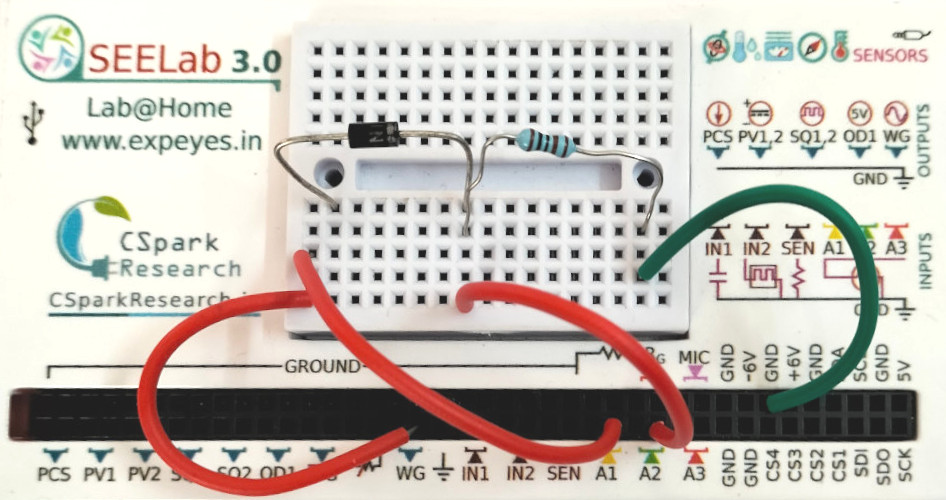
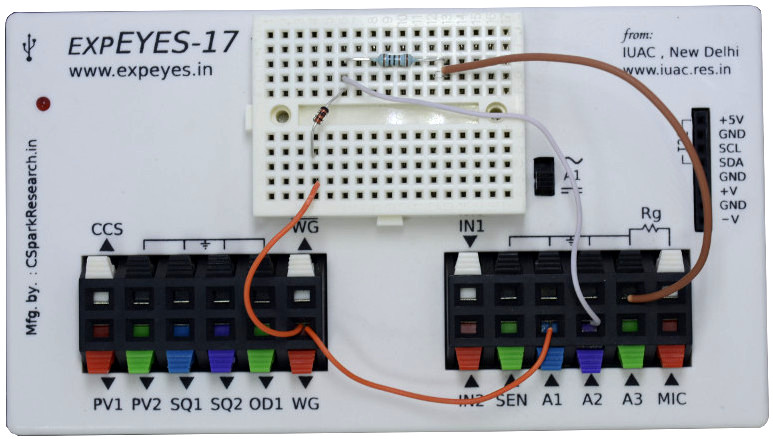
4. Circuit Diagram / Setup
Part A — Basic half-wave rectifier (no filter capacitor):
- Connect the anode of the diode to WG.
- Connect the cathode of the diode to one end of $R_L$.
- Connect the other end of $R_L$ to GND.
- Connect WG to A1 (monitors $V_{in}$).
- Connect the junction of the diode cathode and $R_L$ to A2 (monitors $V_{out}$).
Part B — With RC filter:
- Connect the filter capacitor $C = 1\text{ }\mu F$ in parallel with $R_L$ (between A2 node and GND). Do not add this capacitor until Part A observations are complete.
Note on junction capacitance test: To observe the $C_j$ effect clearly, temporarily remove $R_L$ (open-circuit load) and use a 1N4007 diode at 1000 Hz. The $1\text{ M}\Omega$ input impedance of A2 will allow the reverse-half leakage to become visible.
5. Procedure
Part A — Basic Rectifier
- Open the SEELab3 / ExpEYES app and select the “Half-Wave Rectifier” experiment.
- Set the WG to a sinusoidal output at $f = 1000\text{ Hz}$, amplitude $\approx 3\text{ V}$ peak.
- Click “Start”. Observe both traces:
- A1 — the input sinusoidal voltage
- A2 — the rectified output across $R_L$
- Note the following from the display:
- The peak amplitude of A2 compared to A1 — the difference is the diode forward voltage drop $V_f$.
- The input voltage at which the output just begins to appear — this is the cut-in voltage $V_{th}$.
- The shape of the output during the negative half-cycle — it should be near zero (with $R_L$ connected).
- Sketch both waveforms and compare with the ideal textbook picture.
Part B — Junction Capacitance Effect
- Remove $R_L$ from the circuit (open-circuit output). Keep A2 connected directly at the diode cathode.
- Replace the 1N4148 with a 1N4007 diode.
- Observe the A2 trace during the negative half-cycle — a small sinusoidal signal should now be visible, caused by capacitive coupling through $C_j$.
- Restore $R_L = 1\text{ k}\Omega$ and observe that the reverse-half signal disappears.
Part C — RC Filter
- Reconnect the 1N4148 and $R_L = 1\text{ k}\Omega$.
- Connect the filter capacitor $C = 1\text{ }\mu F$ in parallel with $R_L$.
- Observe the A2 trace — the output should now be a near-DC level with a small ripple superimposed.
- Note the ripple amplitude and the average DC level.
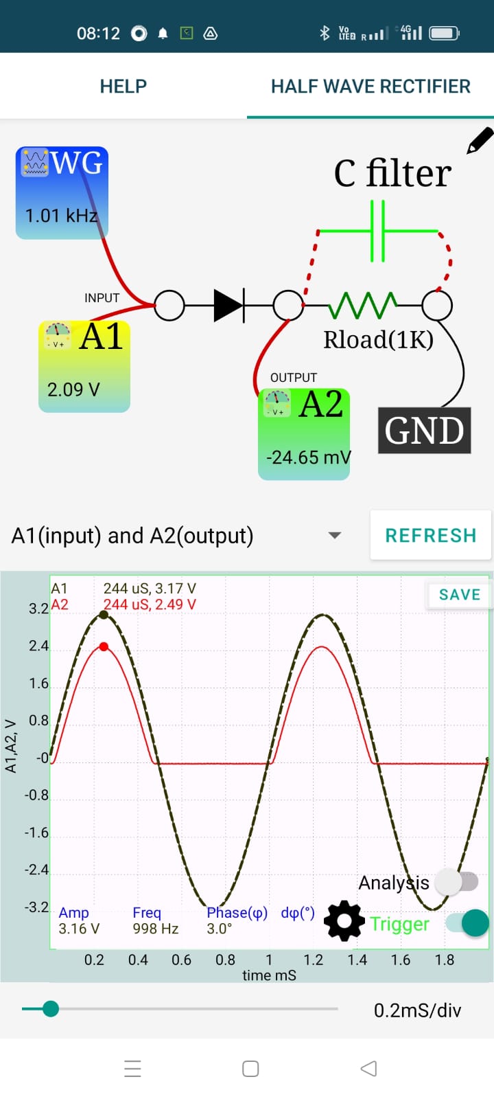
Halfwave (No Filter Capacitor. Notice voltage drop)
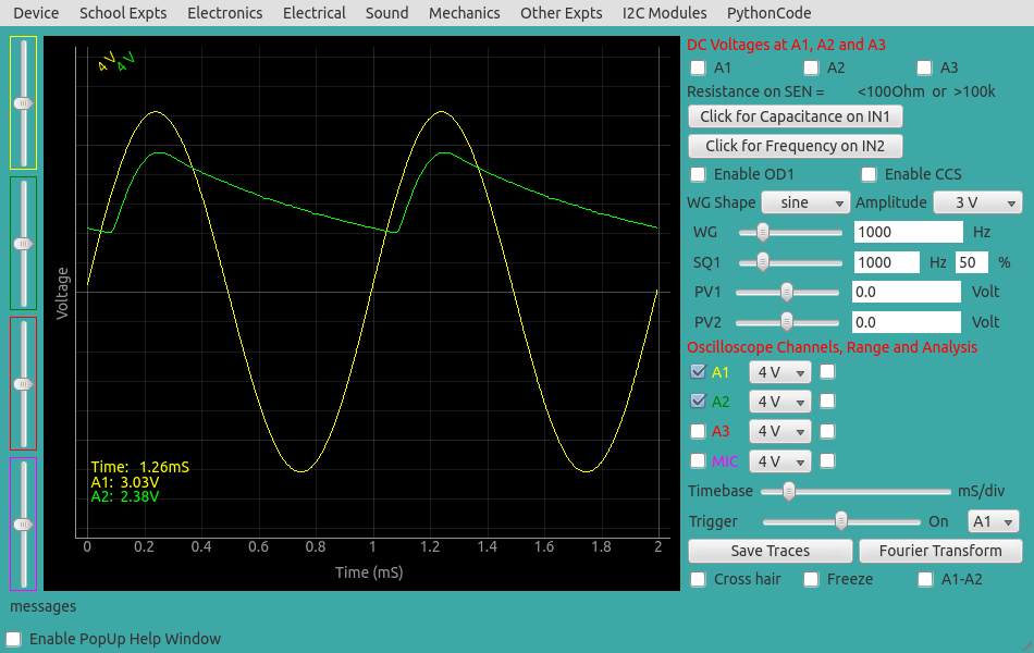
Half Wave With Filter
6. Observation Table
| Diode used: ____ | $R_L$: ____ $\Omega$ | Frequency: ____ Hz |
6a. Part A — Basic Rectifier
| Quantity | Measured Value |
|---|---|
| Input peak voltage $V_{in,\text{peak}}$ (V) | |
| Output peak voltage $V_{out,\text{peak}}$ (V) | |
| Forward voltage drop $V_f = V_{in,\text{peak}} - V_{out,\text{peak}}$ (V) | |
| Cut-in threshold voltage $V_{th}$ (V) | |
| Output voltage during negative half-cycle (V) | |
| Phase of output relative to input | In phase / Inverted |
6b. Part B — Junction Capacitance (no $R_L$, 1N4007 at 1000 Hz)
| Condition | Reverse-half peak voltage at A2 (V) |
|---|---|
| 1N4007, no $R_L$ (open circuit) | |
| 1N4007, $R_L = 1\text{ k}\Omega$ | |
| 1N4148, no $R_L$ (open circuit) |
6c. Part C — RC Filter
| Filter capacitor $C$ | Ripple voltage $V_{ripple}$ (V) | Average output $V_{avg}$ (V) |
|---|---|---|
| None (no capacitor) | ||
| $1\text{ }\mu F$ |
7. Results and Discussion
- The diode conducted only during the positive half-cycle, producing a half-wave rectified output, as expected.
- The output peak was ____ V, which is ____ V less than the input peak of ____ V, consistent with the silicon diode forward voltage drop of $\approx 0.6\text{ V}$.
- The output began appearing only when $V_{in}$ exceeded the cut-in voltage of ____ V, confirming the threshold behavior absent in the ideal textbook model.
- With the 1N4007 and no load resistor, a reverse-half signal of ____ V peak was observed, attributed to capacitive coupling through the $20\text{ pF}$ junction capacitance. Connecting $R_L$ reduced this to ____ V, demonstrating that the effect is suppressed by a low-impedance load.
- Adding a $1\text{ }\mu F$ filter capacitor reduced the ripple from ____ V (no filter) to ____ V, raising the average DC output to ____ V.
8. Precautions
- Diode polarity: Verify the cathode (marked with a band) is connected toward the load ($R_L$) and the anode toward WG. Reversing the diode will block the positive half and pass the negative half instead.
- WG amplitude: Keep the peak input voltage within $\pm 3.3\text{ V}$ to stay within the safe input range of A1 and A2.
- Capacitor sequence: Observe the basic rectifier waveform thoroughly before connecting the filter capacitor — adding it too early masks the individual half-cycle shape.
- Capacitor polarity: If using an electrolytic capacitor for $C$, connect the positive terminal to the A2 (output) node and negative to GND. Reversing it can damage the capacitor.
- Frequency for junction capacitance test: The $C_j$ coupling effect is only visible at high frequencies (≥ 500 Hz). At 50 Hz the reactance of even 20 pF is $\approx 160\text{ M}\Omega$ — far too high to produce a measurable signal.
9. Troubleshooting
| Symptom | Possible Cause | Corrective Action |
|---|---|---|
| A2 shows no output at all | Diode inserted backwards. | Swap the diode orientation; re-check cathode band direction. |
| A2 shows the full sine wave (both halves) | Diode is short-circuited or bypassed; wrong node monitored. | Check breadboard for solder bridges or misplaced wires; confirm A2 is at the cathode–$R_L$ junction. |
| Output peak equals input peak (no $V_f$ drop) | A1 and A2 both connected to same node (before the diode). | Verify A2 is after the diode, not at the WG terminal. |
| Ripple does not reduce after adding capacitor | Capacitor not in parallel with $R_L$, or capacitor is faulty/open. | Confirm capacitor is connected between A2 node and GND; test capacitor with a multimeter. |
| Negative half shows large signal even with $R_L$ connected | $R_L$ not making proper contact in breadboard. | Re-seat $R_L$; verify with multimeter in resistance mode. |
10. Viva-Voce Questions
Q1. What is rectification, and why is a diode suitable for this purpose?
Ans: Rectification is the conversion of an alternating current (AC) — which periodically reverses direction — into a unidirectional (DC) current. A PN junction diode is suitable because it has strongly asymmetric conductance: it offers very low resistance when forward biased (conducts) and very high resistance when reverse biased (blocks). This one-way valve action allows only one half of the AC cycle to reach the load.
Q2. Why does the actual output peak differ from the input peak, and why does conduction not begin at $0\text{ V}$?
Ans: A real silicon diode has a built-in potential barrier of approximately $0.6$–$0.7\text{ V}$ at the junction. The forward-biasing voltage must first overcome this barrier before significant current flows. Consequently: (1) the output does not appear until $V_{in}$ exceeds the cut-in voltage $V_{th} \approx 0.6\text{ V}$, and (2) the conducting portion of the waveform is shifted down by $V_f$, so the output peak $= V_{in,\text{peak}} - V_f$. Ideal diode models in textbooks ignore $V_f$, which is why they show a perfect half-sinusoid starting at $0\text{ V}$.
Q3. What is junction capacitance, and under what conditions does it cause a problem in a rectifier?
Ans: Junction capacitance $C_j$ is a parasitic capacitance that exists across every reverse-biased PN junction, arising from the depletion region acting as a dielectric between two charge layers. During the reverse half-cycle, $C_j$ passes a displacement current $I = C_j \cdot dV/dt$, coupling a small fraction of the input to the output. This becomes significant when: (a) the frequency is high (large $dV/dt$), (b) the diode has a large $C_j$ (e.g., 1N4007 at 20 pF), and (c) the load impedance is high (no $R_L$ to discharge the coupled charge). At mains frequency (50 Hz) with a 1 k$\Omega$ load, the effect is completely negligible.
Q4. Explain how a filter capacitor reduces the ripple in the rectified output.
Ans: When the diode conducts (positive half-cycle), the capacitor charges rapidly to the peak output voltage $V_{peak}$. When the diode stops conducting (negative half-cycle), instead of the output falling to zero, the capacitor discharges slowly through $R_L$ with a time constant $\tau = R_L C$. If $\tau \gg T$ (the period of the AC signal), the voltage hardly falls before the next positive peak recharges the capacitor — the output becomes a nearly smooth DC level with a small exponential ripple superimposed. The larger the $RC$ product, the smaller the ripple.
Q5. What are the disadvantages of a half-wave rectifier compared to a full-wave rectifier?
Ans: Three main disadvantages: (1) Low average output voltage — the average DC value of a half-wave rectified sine is $V_{avg} = V_{peak}/\pi \approx 0.318\,V_{peak}$, compared to $2V_{peak}/\pi \approx 0.636\,V_{peak}$ for full-wave. (2) High ripple — the ripple frequency equals the input frequency $f$, requiring a larger filter capacitor for the same smoothing compared to full-wave rectification where the ripple frequency is $2f$. (3) Poor transformer utilization — the transformer core carries DC-biased current, increasing hysteresis losses and reducing efficiency.