Experiment: Clipping Circuit Using a PN Junction Diode
1. Aim
To study the action of a diode clipping circuit — a circuit that removes (clips) the portion of an AC waveform that exceeds a set voltage level — and to observe how the clipping level shifts when the DC bias on the diode is varied using the programmable source PV1.
2. Apparatus / Components Required
- SEELab3 unit
- PN junction diode (1N4148)
- Resistor $R = 1\text{ k}\Omega$
- Connecting wires
- PC or Smartphone with SEELab3 software
3. Theory & Principle
3.1 Clipping Action
A clipper (or limiter) circuit passes the input signal unchanged as long as it stays within a defined voltage window, and flattens (clips) it to a fixed level once it crosses that threshold.
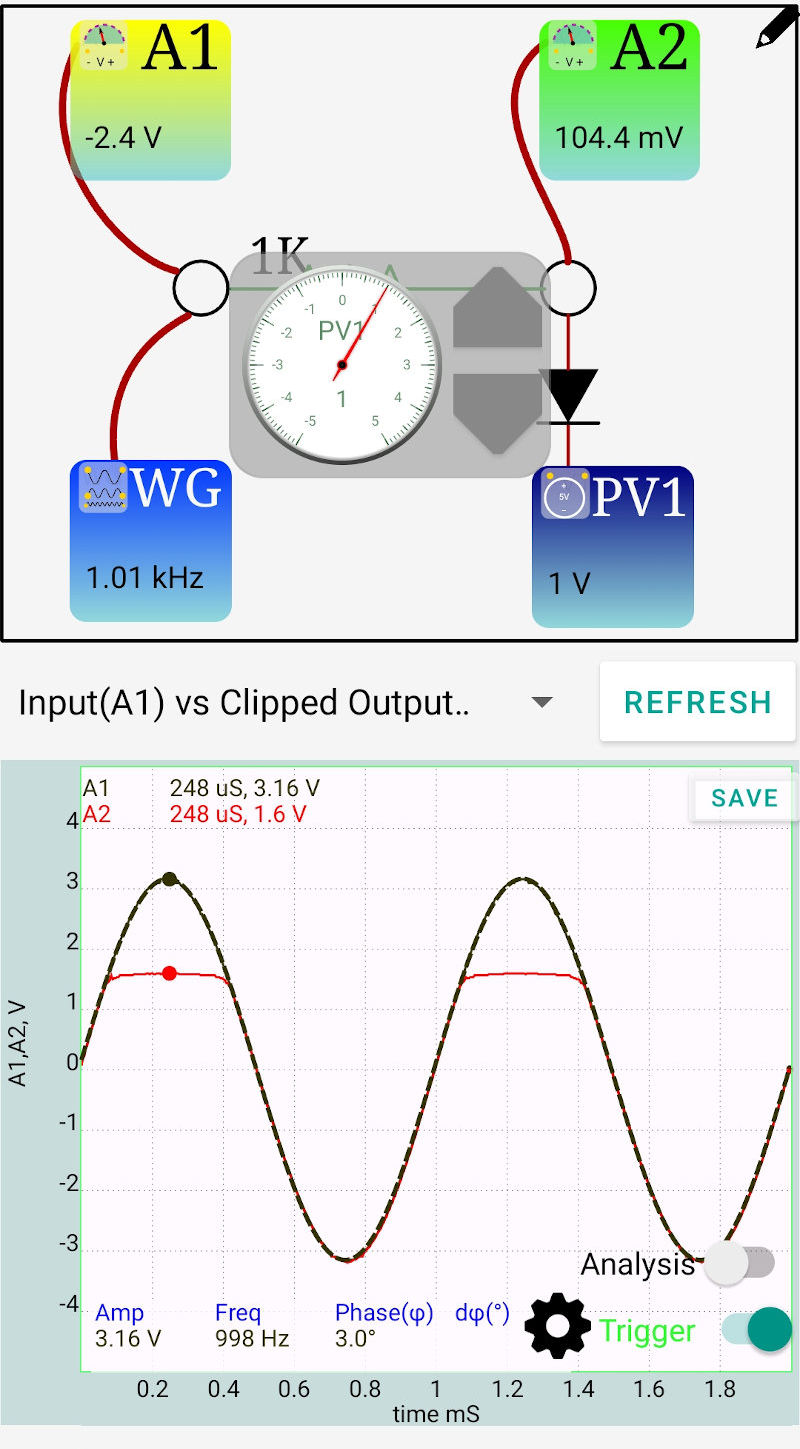
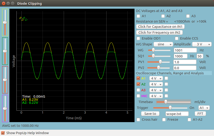
In the circuit here, $R$ and the diode form a series path from WG to PV1. Channel A2 monitors the voltage at the junction between $R$ and the diode anode — i.e., the output node.
When the input swings positive and the output node voltage tries to rise above $V_{clip}$, the diode becomes forward biased and clamps the output to:
\[V_{clip} = V_{PV1} + V_f \approx V_{PV1} + 0.6\text{ V}\]Excess current is diverted through the diode into PV1 rather than appearing across the output. Below $V_{clip}$ the diode is reverse biased and the output follows the input (reduced slightly by the $R$–load divider).
Setting PV1 = 0 V gives $V_{clip} \approx +0.6\text{ V}$ (one diode drop above ground).
Raising PV1 raises the clipping level proportionally — the diode does not conduct until the output reaches $V_{PV1} + V_f$.
3.2 Negative Clipping
Reversing the diode direction flips the circuit so the diode conducts on the negative half-cycle instead. The clipping level becomes:
\[V_{clip,\text{neg}} = V_{PV1} - V_f\]Applying a negative voltage to PV1 with the reversed diode clips the negative half at a programmable level below zero.
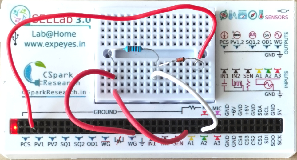
4. Circuit Diagram / Setup
- Connect WG to one end of $R$ ($1\text{ k}\Omega$).
- Connect the other end of $R$ to the anode of the diode. This junction is the output node — connect it to A2.
- Connect the cathode of the diode to PV1.
- Connect WG also to A1 to monitor the input.
For negative clipping: reverse the diode (cathode to $R$, anode to PV1) and set PV1 to a negative value.
5. Procedure
Part A — Positive clipping, variable level
- Open the SEELab3 app. Set WG to a sinusoidal signal at $f = 1000\text{ Hz}$, amplitude $\approx 3\text{ V}$ peak.
- Set PV1 = 0 V. Click “Start” and observe A1 (input) and A2 (output).
- The positive peaks of A2 should be clipped flat at $\approx +0.6\text{ V}$; the negative half should follow the input.
- Increase PV1 in steps: 0.5 V, 1.0 V, 1.5 V, 2.0 V. At each step note the clipping level on A2 and confirm it tracks $V_{PV1} + 0.6\text{ V}$.
- Set PV1 high enough (e.g., $> 3\text{ V}$) that clipping disappears entirely — the output should now follow the full input waveform.
Part B — Negative clipping
- Reverse the diode in the breadboard (cathode to $R$, anode to PV1).
- Set PV1 to 0 V and observe — the negative peaks are now clipped at $\approx -0.6\text{ V}$.
- Set PV1 to −0.5 V, −1.0 V, −1.5 V (negative values) and record the clipping level each time.
Mobile App
Desktop App
6. Observation Table
| $R$: ____ $\Omega$ | Frequency: ____ Hz | $V_{in,\text{peak}}$: ____ V |
6a. Part A — Positive Clipping
| PV1 setting (V) | Theoretical $V_{clip} = V_{PV1} + 0.6$ (V) | Measured $V_{clip}$ at A2 (V) | Error (V) |
|---|---|---|---|
| 0.0 | 0.6 | ||
| 0.5 | 1.1 | ||
| 1.0 | 1.6 | ||
| 1.5 | 2.1 | ||
| 2.0 | 2.6 |
6b. Part B — Negative Clipping (diode reversed)
| PV1 setting (V) | Theoretical $V_{clip} = V_{PV1} - 0.6$ (V) | Measured $V_{clip}$ at A2 (V) | Error (V) |
|---|---|---|---|
| 0.0 | −0.6 | ||
| −0.5 | −1.1 | ||
| −1.0 | −1.6 | ||
| −1.5 | −2.1 |
7. Results and Discussion
- With PV1 = 0 V and the diode in the forward orientation, the positive peaks were clipped at ____ V, agreeing with the expected $V_f \approx 0.6\text{ V}$.
- As PV1 was increased, the clipping level rose by the same amount, confirming $V_{clip} = V_{PV1} + V_f$.
- With the diode reversed and PV1 set to negative values, the negative half was clipped at programmable levels below zero, verifying $V_{clip} = V_{PV1} - V_f$.
- The unclipped half of the waveform reproduced the input faithfully, confirming that the diode is fully off (reverse biased) during that half-cycle.
8. Precautions
- PV1 polarity: SEELab3’s PV1 may not support negative voltages on all firmware versions. Check the specification before attempting Part B; if unavailable, Part B can be demonstrated with PV1 = 0 V and diode reversed (clips at $-V_f$).
- Resistor is essential: The series resistor $R$ limits the current through the diode when it clamps. Never omit it — a direct WG-to-diode connection with no $R$ will draw excessive current from the WG output stage.
- Input amplitude: Keep $V_{in,\text{peak}} \leq 3\text{ V}$ to stay within the safe input range of A1 and A2.
- Diode orientation check: Before powering on, confirm the diode orientation with a multimeter in diode-test mode — it is easy to inadvertently reverse the diode when switching between Part A and Part B.
9. Troubleshooting
| Symptom | Possible Cause | Corrective Action |
|---|---|---|
| No clipping — A2 identical to A1 | Diode is reversed (blocking, not clamping) or open-circuit. | Swap diode orientation; test diode with multimeter. |
| Both halves clipped | Two diodes in circuit by mistake, or $R$ shorted. | Check breadboard for stray connections; remove extra components. |
| Clipping level does not shift with PV1 | PV1 not connected to diode cathode, or PV1 output not functioning. | Verify PV1 terminal wiring; check PV1 voltage with A1 channel directly. |
| Clipped level is much higher than $V_{PV1} + 0.6\text{ V}$ | $R$ value too large causing a significant voltage divider drop before clipping. | Reduce $R$ or account for the divider effect in the calculation. |
10. Viva-Voce Questions
Q1. What is a clipper circuit and how does it differ from a rectifier?
Ans: A clipper removes the portion of a waveform that exceeds a set voltage level, leaving the rest unchanged. A rectifier also uses a diode, but its purpose is different — it passes one entire half-cycle and blocks the other, converting AC to pulsating DC. In a clipper, the clipping level is set by a bias voltage and can be placed anywhere on the waveform; the signal below the threshold passes through unaltered. A rectifier is essentially a special case of a clipper where the clipping level is set to $0\text{ V}$ (ground).
Q2. Why does the clipping level equal $V_{PV1} + V_f$ and not simply $V_{PV1}$?
Ans: The diode begins conducting when the voltage at its anode exceeds the voltage at its cathode by $V_f \approx 0.6\text{ V}$. The cathode is held at $V_{PV1}$ by the programmable source. Therefore the diode turns on — and clamps the output — when the output node reaches $V_{PV1} + V_f$. If $V_f$ were zero (ideal diode), the clipping level would equal $V_{PV1}$ exactly.
Q3. What happens to the clipped portion of the signal? Where does that energy go?
Ans: When the output tries to exceed $V_{clip}$, the diode conducts and the excess current flows from the WG source, through $R$, through the forward-biased diode, and into PV1. The resistor $R$ drops the excess voltage ($V_{in} - V_{clip}$) across itself as heat. The signal energy in the clipped portion is therefore dissipated in $R$ — none of it reaches the output node, which is why the output appears flat at $V_{clip}$.
Q4. How would you design a circuit that clips both the positive and negative peaks simultaneously (a double clipper)?
Ans: Place two diodes in anti-parallel (back-to-back, opposite orientations) between the output node and ground — or between the output node and two separate DC bias sources ($+V_{clip,1}$ and $-V_{clip,2}$). D1 (anode to output, cathode to $+V_{clip,1}$) clamps the positive peak, and D2 (cathode to output, anode to $-V_{clip,2}$) clamps the negative peak. This is also called a limiter and is used in audio circuits and protection stages to prevent signals from exceeding a safe voltage window.
Q5. A clipper and a Zener diode voltage regulator both limit voltage. What is the key difference?
Ans: A clipper uses a forward-biased PN junction — its clamp voltage is $V_{PV1} + V_f$, which is set by an external bias and is adjustable. A Zener regulator uses the reverse breakdown (Zener) voltage of a specially doped diode, which is a fixed property of the device (e.g., 3.3 V, 5.1 V, 12 V). The Zener conducts heavily in reverse once $V_Z$ is exceeded, clamping the voltage without needing an external bias supply. Clippers are used for waveform shaping; Zener regulators are used for voltage stabilisation.