Experiment: Clamping Circuit Using a PN Junction Diode
1. Aim
To study the action of a diode clamping circuit — a circuit that shifts the entire AC waveform up or down by adding a DC offset — and to observe how the clamped output level is controlled by the DC bias applied through PV1.
2. Apparatus / Components Required
- SEELab3 unit
- PN junction diode (1N4148)
- Capacitor $C = 1\text{ }\mu F$
- Connecting wires
- PC or Smartphone with SEELab3 software
3. Theory & Principle
3.1 Clipper vs Clamper — the key distinction
A clipper (previous experiment) cuts away part of the waveform — the shape of the surviving portion is unchanged but some of it is removed. A clamper shifts the entire waveform up or down without altering its shape — the peak-to-peak amplitude is preserved, only the DC level changes.
Mobile App
Desktop App
3.2 How the clamper works
The circuit consists of a series capacitor $C$ between WG and the output node, with a diode connecting the output node to PV1.
On the first negative peak of the input, the output node is pulled low and the diode becomes forward biased, clamping the output node to:
\[V_{clamp} = V_{PV1} - V_f \approx V_{PV1} - 0.6\text{ V}\]The capacitor charges rapidly to the difference $V_{in,\text{neg_peak}} - V_{clamp}$ and holds this charge. On subsequent cycles the capacitor’s stored voltage acts as a DC offset, shifting the entire waveform upward so that the negative peaks sit at $V_{clamp}$.
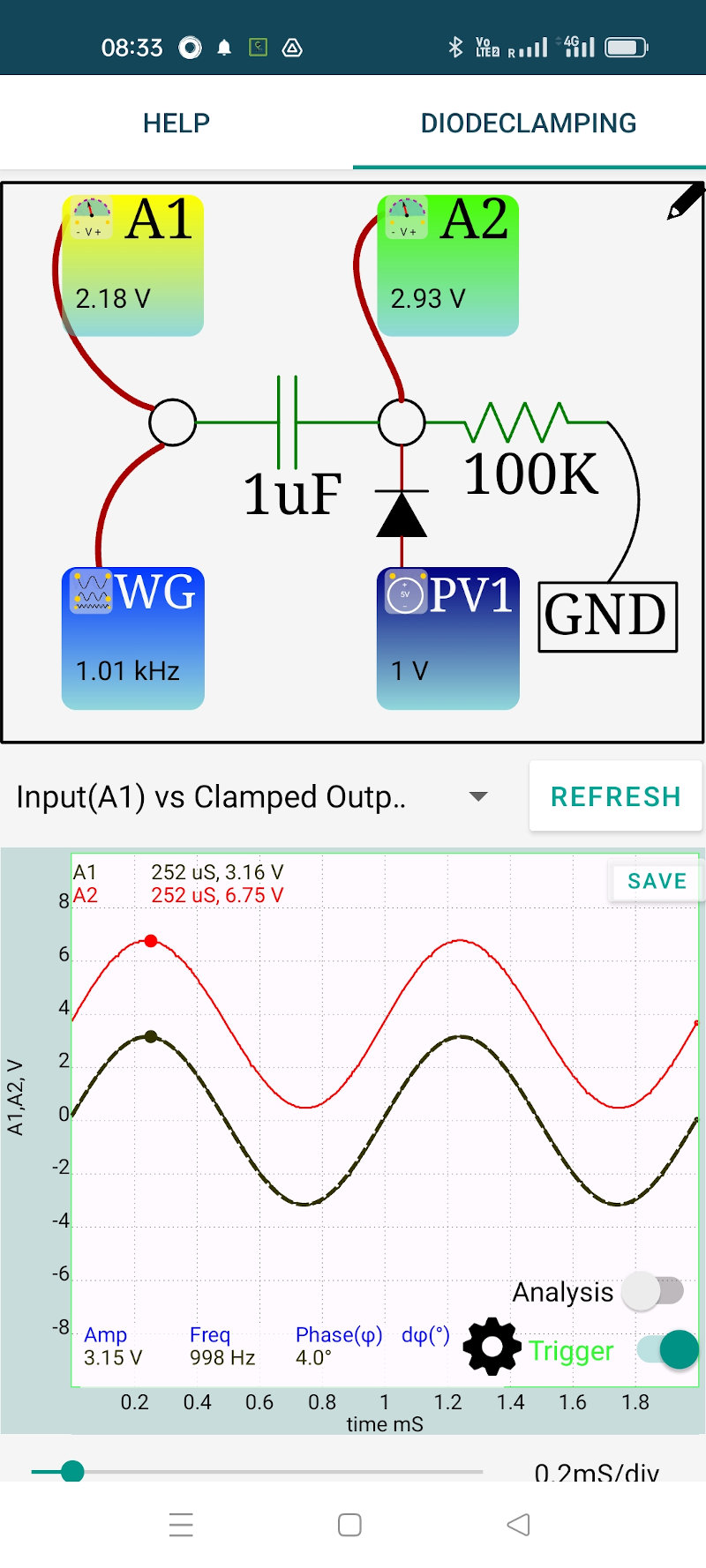
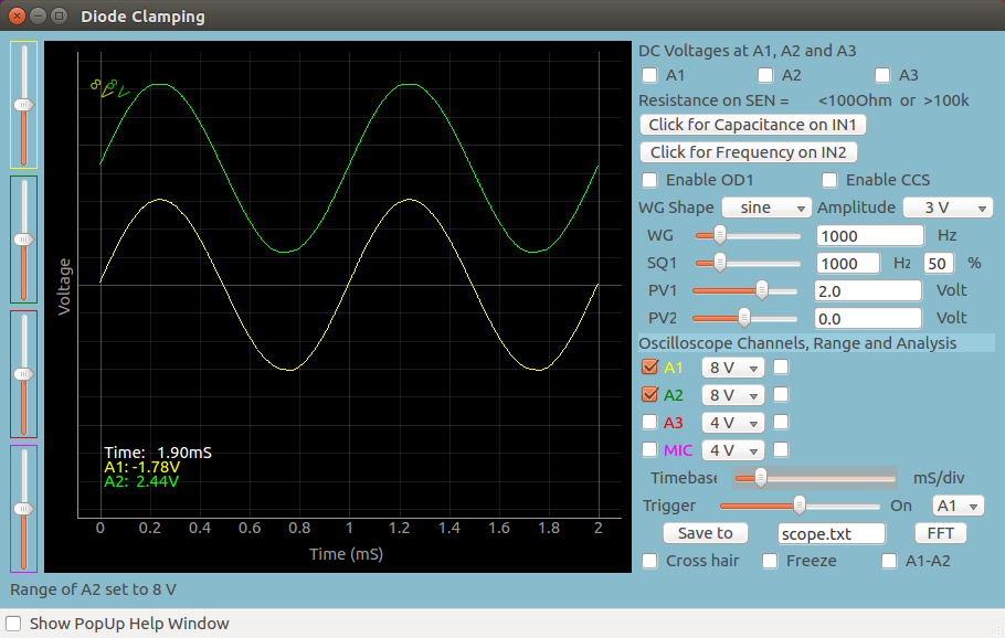
For a $3\text{ V}$ peak sinusoid and $V_{PV1} = 1\text{ V}$:
\[V_{clamp} = 1.0 - 0.6 = 0.4\text{ V} \approx 0.3\text{ V (measured)}\]The entire waveform is lifted so its lowest point sits at $\approx +0.3\text{ V}$, and the positive peak rises to $\approx 0.3 + 6 = 6.3\text{ V}$ (peak-to-peak preserved at $6\text{ V}$).
Important: The output peak-to-peak voltage equals the input peak-to-peak — the clamper adds DC offset only. This is what distinguishes it from a clipper, which reduces peak-to-peak.
3.3 Reverse clamping
Reversing the diode flips the action — the diode now clamps the positive peaks instead of the negative ones, shifting the entire waveform downward. Applying a negative voltage to PV1 with the reversed diode clamps the positive peaks below zero.
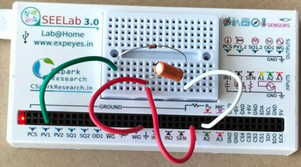
4. Circuit Diagram / Setup
- Connect WG to one plate of capacitor $C$ ($1\text{ }\mu F$). Connect A1 to WG to monitor the input.
- Connect the other plate of $C$ to the anode of the diode. This is the output node — connect it to A2.
- Connect the cathode of the diode to PV1.
For reverse clamping: swap the diode (cathode to output node, anode to PV1) and apply negative voltages on PV1.
5. Procedure
Part A — Positive (upward) clamping
- Open the SEELab3 app. Set WG to a sinusoidal output at $f = 1000\text{ Hz}$, amplitude $\approx 3\text{ V}$ peak.
- Set PV1 = 1 V. Click “Start” and observe A1 and A2.
- A1 shows the original symmetric sinusoid centred on $0\text{ V}$.
- A2 should show the same waveform shifted upward — negative peaks lifted to $\approx V_{PV1} - 0.6\text{ V}$.
- Confirm the peak-to-peak amplitude of A2 equals that of A1.
- Vary PV1: 0 V, 0.5 V, 1.0 V, 1.5 V, 2.0 V. Record the clamped negative-peak level each time.
Part B — Reverse (downward) clamping
- Reverse the diode and set PV1 to negative values: 0 V, −0.5 V, −1.0 V, −1.5 V.
- Observe that the positive peaks are now clamped and the waveform shifts downward.
- Record the clamped positive-peak level at each PV1 setting.
6. Observation Table
| Frequency: ____ Hz | $V_{in,\text{peak}}$: ____ V | $V_{in,\text{p-p}}$: ____ V |
6a. Part A — Positive Clamping
| PV1 (V) | Theoretical $V_{neg_peak} = V_{PV1} - 0.6$ (V) | Measured $V_{neg_peak}$ (V) | Measured $V_{p\text{-}p}$ at A2 (V) |
|---|---|---|---|
| 0.0 | −0.6 | ||
| 0.5 | 0.9 | ||
| 1.0 | 0.4 | ||
| 1.5 | 0.9 | ||
| 2.0 | 1.4 |
6b. Part B — Reverse Clamping (diode reversed)
| PV1 (V) | Theoretical $V_{pos_peak} = V_{PV1} + 0.6$ (V) | Measured $V_{pos_peak}$ (V) | Measured $V_{p\text{-}p}$ at A2 (V) |
|---|---|---|---|
| 0.0 | 0.6 | ||
| −0.5 | 0.1 | ||
| −1.0 | −0.4 | ||
| −1.5 | −0.9 |
7. Results and Discussion
- With PV1 = 1 V, the negative peaks of the output were clamped to ____ V, against a theoretical value of $1.0 - 0.6 = 0.4\text{ V}$.
- The peak-to-peak amplitude at A2 was ____ V, equal to the input peak-to-peak of ____ V, confirming that the clamper preserves waveform shape and only shifts the DC level.
- As PV1 was increased, the clamped level rose proportionally — each $1\text{ V}$ increase in PV1 raised the output by $1\text{ V}$, verifying $V_{clamp} = V_{PV1} - V_f$.
- With the diode reversed and PV1 negative, the waveform shifted downward symmetrically, confirming that the clamping direction is controlled entirely by diode orientation and PV1 polarity.
8. Precautions
- Capacitor value: The capacitor must fully charge within the first few cycles for steady-state clamping to be established. For $f = 1000\text{ Hz}$, $C = 1\text{ }\mu F$ with the $1\text{ M}\Omega$ input impedance of A2 gives $\tau = RC = 1\text{ s}$ — very long. In practice the diode provides a fast charge path on the clamping half-cycle; however, the discharge through $1\text{ M}\Omega$ is slow, which is what holds the DC shift. Do not add a low-value load resistor across the output — it will discharge the capacitor too quickly and degrade the clamping action.
- A2 input impedance dependence: The clamped DC level depends on the $1\text{ M}\Omega$ input impedance of A2 holding the capacitor charge between cycles. With a real load (e.g., $10\text{ k}\Omega$) the clamping will degrade — the practical clamper needs a buffer amplifier for low-impedance loads.
- Allow settling: The output takes a few cycles to settle to steady-state after changing PV1. Wait briefly before recording measurements.
- Capacitor polarity: If an electrolytic capacitor is used, it must be oriented correctly. Preferred: use a non-polarised film or ceramic capacitor for this experiment.
9. Troubleshooting
| Symptom | Possible Cause | Corrective Action |
|---|---|---|
| A2 shows same waveform as A1 — no DC shift | Capacitor missing, shorted, or not making contact. | Verify capacitor is in series between WG and the output node; test with multimeter. |
| DC shift present but waveform is distorted | Diode is in wrong orientation — clipping instead of clamping. | Check diode direction; in Part A the anode goes to the output node, cathode to PV1. |
| Clamped level drifts slowly | Capacitor discharging through A2’s $1\text{ M}\Omega$ impedance between cycles at low frequency. | Increase frequency to 1000 Hz or above so the period is much shorter than $\tau = RC$. |
| Peak-to-peak at A2 is smaller than at A1 | Clipper behaviour — a resistor may be accidentally in series, or wrong circuit built. | Confirm no series resistor is present; a pure clamper has only $C$ and the diode. |
10. Viva-Voce Questions
Q1. What is the fundamental difference between a clipper and a clamper?
Ans: A clipper removes part of the waveform — it reduces the peak-to-peak amplitude by cutting away anything above or below a threshold. A clamper shifts the entire waveform up or down by adding a DC offset — the waveform shape and peak-to-peak amplitude are completely preserved. You can verify this instantly from the oscilloscope: if $V_{p\text{-}p}$ at the output equals $V_{p\text{-}p}$ at the input, it is a clamper; if it is smaller, it is a clipper.
Q2. What role does the capacitor play in the clamping circuit?
Ans: The capacitor serves as a DC-blocking and charge-storage element. On the first clamping half-cycle, the diode conducts and the capacitor charges to the difference between the input peak and the clamping voltage. This stored charge acts as a battery — it adds a fixed DC voltage in series with the AC signal on every subsequent cycle, effectively shifting the entire waveform. The capacitor must retain its charge between cycles (i.e., the discharge time constant $\tau = R_{load}C$ must be much larger than the signal period) for steady clamping to be maintained.
Q3. Why is the clamped level $V_{PV1} - V_f$ rather than $V_{PV1}$?
Ans: The diode conducts when its anode (output node) is more positive than its cathode (PV1) by $V_f \approx 0.6\text{ V}$. It stops conducting — and therefore clamps — when the output node reaches exactly $V_{PV1} - V_f$ during the negative peak, not $V_{PV1}$. The $V_f$ drop across the forward-biased diode subtracts from the bias, so the final clamped level is always one diode drop below (for this orientation) the applied bias voltage.
Q4. The positive peak of the clamped output is much higher than the original input peak. Is this a problem?
Ans: Not a circuit problem — it is the expected behaviour. If the negative peak is lifted by $\Delta V$ (the DC shift), the positive peak is also lifted by the same $\Delta V$, since the entire waveform shifts rigidly. For a $3\text{ V}$ peak input clamped at $+0.4\text{ V}$, the positive peak reaches $0.4 + 6 = 6.4\text{ V}$ — well above the original $+3\text{ V}$. Practically, this means the downstream circuit (and the A2 input channel) must be able to handle this elevated positive swing without clipping or damage.
Q5. Where is clamping used in real electronic systems?
Ans: Clampers appear in several practical applications: (1) Television sync restoration — the sync tip of a composite video signal is clamped to a reference level at the start of each line to remove noise-induced DC wander. (2) Voltage multiplier circuits — cascaded clampers and peak detectors (Cockcroft-Walton ladder) progressively stack DC offsets to multiply a low AC voltage to a high DC voltage without a transformer. (3) Coupling with level shifting — when an AC signal from one stage needs to be shifted to a specific DC operating point before entering the next stage.