Experiment: Astable Multivibrator Using IC 555
1. Aim
To wire the IC 555 timer in astable (free-running) mode, to measure the output frequency and duty cycle, and to verify the theoretical values predicted by the RC component values using SEELab3.
2. Apparatus / Components Required
- SEELab3 or ExpEYES-17 unit
- IC 555 timer
- Resistors: $R_1 = 2.2\text{ k}\Omega$, $R_2 = 1\text{ k}\Omega$
- Capacitor $C = 1\text{ }\mu F$ (timing), $C_{bypass} = 0.01\text{ }\mu F$ (pin 5 to GND, noise suppression)
- DC supply: $5\text{ V}$ (or $V_{CC}$ from SEELab3)
- Breadboard and connecting wires
- PC or Smartphone with SEELab3 / ExpEYES software
3. Theory & Principle
3.1 The 555 in Astable Mode
In astable mode the 555 has no stable state — its output continuously oscillates between HIGH ($\approx V_{CC}$) and LOW ($\approx 0\text{ V}$) without any external trigger. The timing is set entirely by $R_1$, $R_2$, and $C$.
Internally, the 555 contains a voltage divider that sets two thresholds: the upper threshold at $\frac{2}{3}V_{CC}$ and the lower threshold at $\frac{1}{3}V_{CC}$. The capacitor $C$ charges through $R_1 + R_2$ and discharges through $R_2$ alone, cycling between these two thresholds indefinitely.

3.2 Timing Equations
The charge time (output HIGH) while $C$ charges from $\frac{1}{3}V_{CC}$ to $\frac{2}{3}V_{CC}$ through $R_1 + R_2$:
\[t_{HIGH} = 0.693 \times (R_1 + R_2) \times C\]The discharge time (output LOW) while $C$ discharges from $\frac{2}{3}V_{CC}$ to $\frac{1}{3}V_{CC}$ through $R_2$:
\[t_{LOW} = 0.693 \times R_2 \times C\]The total period and frequency:
\[T = t_{HIGH} + t_{LOW} = 0.693 \times (R_1 + 2R_2) \times C\] \[\boxed{f = \frac{1}{T} = \frac{1.443}{(R_1 + 2R_2) \times C}}\]The duty cycle (fraction of period the output is HIGH):
\[\boxed{D = \frac{t_{HIGH}}{T} = \frac{R_1 + R_2}{R_1 + 2R_2}}\]Worked example (ExpEYES-17 values): $R_1 = 2.2\text{ k}\Omega$, $R_2 = 1\text{ k}\Omega$, $C = 1\text{ }\mu F$: \(f = \frac{1.443}{(2200 + 2000) \times 10^{-6}} = 343.6\text{ Hz}, \quad D = \frac{3200}{4200} = 76.2\%\)
Because the capacitor charges through $R_1 + R_2$ but discharges through $R_2$ only, $t_{HIGH} > t_{LOW}$ always — the duty cycle is always above 50% in the standard astable configuration.
3.3 Pin Functions (IC 555)
| Pin | Name | Function in Astable Mode |
|---|---|---|
| 1 | GND | Ground |
| 2 | Trigger | Tied to pin 6 (threshold) |
| 3 | Output | Square wave output — connect to A1 |
| 4 | Reset | Tied to $V_{CC}$ (disabled) |
| 5 | Control | $0.01\text{ }\mu F$ to GND (noise bypass) |
| 6 | Threshold | Top of capacitor $C$ — connect to A2 |
| 7 | Discharge | Junction of $R_1$ and $R_2$ |
| 8 | $V_{CC}$ | Supply voltage ($5$–$15\text{ V}$) |
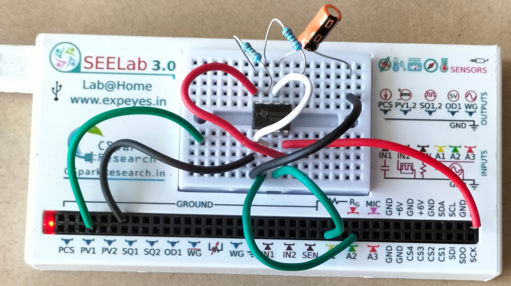
4. Circuit Diagram / Setup
- Wire the IC 555 on the breadboard following the schematic in §3.
- Connect $R_1$ between $V_{CC}$ and pin 7 (discharge).
- Connect $R_2$ between pin 7 and pin 6/2 (threshold/trigger, tied together).
- Connect $C$ between pin 6/2 and GND.
- Connect $C_{bypass}$ ($0.01\text{ }\mu F$) between pin 5 and GND.
- Tie pin 4 (reset) to $V_{CC}$.
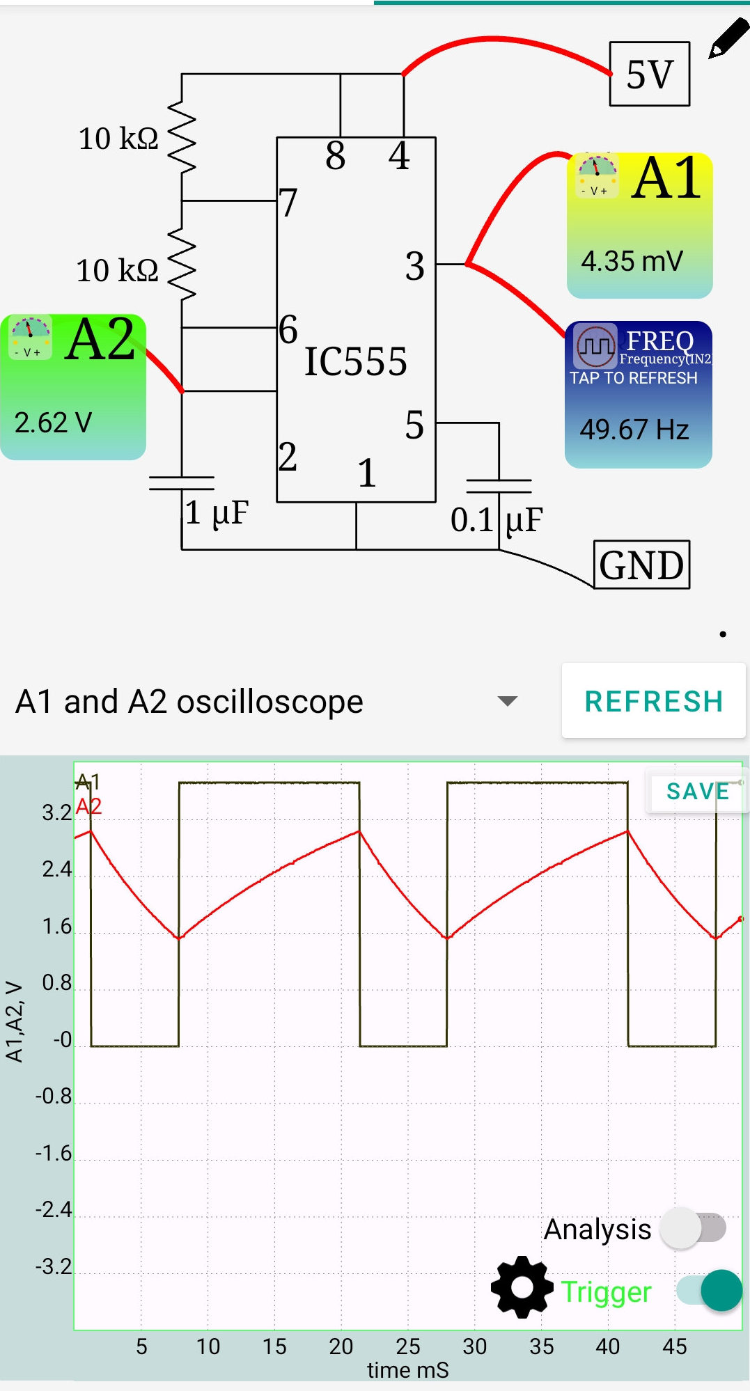
- A1 monitors pin 3 (output square wave). Also connect pin 3 to IN2 for frequency and duty cycle measurement.
- A2 monitors pin 6 (capacitor voltage — the sawtooth charging waveform).
5. Procedure
- Open the SEELab3 / ExpEYES app and navigate to the “IC 555 Astable” experiment or use the oscilloscope directly.
- Power the 555 from $V_{CC}$ ($5\text{ V}$). The output on A1 should immediately begin toggling — no trigger is needed.
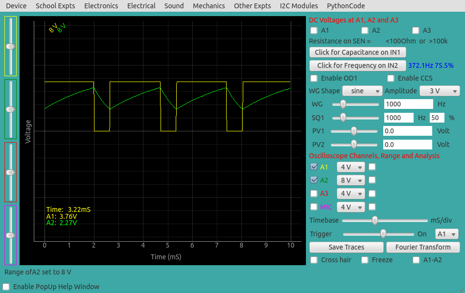
- Observe A1 (square wave) and A2 (capacitor sawtooth) simultaneously. Confirm:
- A1 switches between $\approx 0\text{ V}$ and $\approx V_{CC}$.
- A2 oscillates between $\frac{1}{3}V_{CC}$ and $\frac{2}{3}V_{CC}$.
- A1 goes HIGH when A2 reaches $\frac{1}{3}V_{CC}$, and LOW when A2 reaches $\frac{2}{3}V_{CC}$.
- Read the frequency and duty cycle from the IN2 measurement display.
- Compare with the theoretical values calculated from the formulae in §3.2.
- Component variation: Swap $R_1$, $R_2$, or $C$ for different values and record how frequency and duty cycle change. Use the online 555 calculator to predict values before measuring.
Mobile App
Desktop App
6. Observation Table
| $V_{CC}$: ____ V | $\frac{1}{3}V_{CC}$: ____ V | $\frac{2}{3}V_{CC}$: ____ V |
6a. Verification with Standard Values ($R_1 = 2.2\text{ k}\Omega$, $R_2 = 1\text{ k}\Omega$, $C = 1\text{ }\mu F$)
| Quantity | Formula | Theoretical | Measured |
|---|---|---|---|
| $t_{HIGH}$ (ms) | $0.693(R_1+R_2)C$ | ||
| $t_{LOW}$ (ms) | $0.693\, R_2\, C$ | ||
| Period $T$ (ms) | $t_{HIGH} + t_{LOW}$ | ||
| Frequency $f$ (Hz) | $1.443\,/\,(R_1+2R_2)C$ | 343.6 | |
| Duty cycle $D$ (%) | $(R_1+R_2)\,/\,(R_1+2R_2)$ | 76.2 | |
| $V_{cap,\,min}$ at A2 (V) | $\frac{1}{3}V_{CC}$ | ||
| $V_{cap,\,max}$ at A2 (V) | $\frac{2}{3}V_{CC}$ |
6b. Component Variation
| $R_1$ ($\Omega$) | $R_2$ ($\Omega$) | $C$ ($\mu$F) | Theoretical $f$ (Hz) | Measured $f$ (Hz) | Theoretical $D$ (%) | Measured $D$ (%) |
|---|---|---|---|---|---|---|
| 2200 | 1000 | 1.0 | 343.6 | 76.2 | ||
| 2200 | 2200 | 1.0 | ||||
| 4700 | 1000 | 1.0 | ||||
| 2200 | 1000 | 0.1 |
7. Results and Discussion
- The 555 produced a continuous square wave without any external trigger, confirming astable operation.
- At $R_1 = 2.2\text{ k}\Omega$, $R_2 = 1\text{ k}\Omega$, $C = 1\text{ }\mu F$, the measured frequency was ____ Hz against a theoretical value of $343.6\text{ Hz}$ — a discrepancy of ____ %, consistent with the $\pm 5\%$ tolerance of the resistors and $\pm 20\%$ of the capacitor.
- The capacitor voltage at A2 oscillated between ____ V and ____ V, in close agreement with $\frac{1}{3}V_{CC}$ and $\frac{2}{3}V_{CC}$.
- The duty cycle was always above 50%, as expected, because $R_1 > 0$ always makes $t_{HIGH} > t_{LOW}$.
- Increasing $C$ by 10× reduced the frequency by approximately 10×, confirming the inverse proportionality $f \propto 1/C$.
8. Precautions
- Pin 4 must be HIGH: Pin 4 (Reset) is active-LOW. If left floating it may pick up noise and reset the oscillator unpredictably. Always tie it firmly to $V_{CC}$.
- Pin 5 bypass capacitor: The $0.01\text{ }\mu F$ from pin 5 to GND suppresses power-supply noise on the internal voltage divider. Omitting it can cause jitter in the output frequency, especially at high frequencies or on a noisy supply.
- Supply voltage: The 555 operates from $5\text{ V}$ to $15\text{ V}$. The output HIGH level is approximately $V_{CC} - 1.5\text{ V}$. At $5\text{ V}$ supply the output swings $0$–$3.5\text{ V}$, which is within the safe input range of A1.
- Component tolerance: Standard resistors ($\pm 5\%$) and electrolytic capacitors ($\pm 20\%$) will cause measured frequency to differ from theoretical by up to $\sim 25\%$ in the worst case. Use $1\%$ metal-film resistors and a measured capacitor value for closer agreement.
- Duty cycle cannot reach 50% with the standard astable configuration because $R_1$ is always in the charge path. To achieve 50% duty cycle, place a diode in parallel with $R_2$ so the capacitor charges only through $R_1$.
9. Troubleshooting
| Symptom | Possible Cause | Corrective Action |
|---|---|---|
| No output — A1 stuck HIGH or LOW | Pin 4 (Reset) floating or tied LOW. | Connect pin 4 firmly to $V_{CC}$. |
| Output frequency much lower than expected | Capacitor value much larger than intended (e.g., electrolytic marked $\mu F$ but actually $mF$). | Measure capacitor with LCR meter; verify marking. |
| Frequency is correct but waveform is noisy/jittery | Pin 5 bypass capacitor missing. | Add $0.01\text{ }\mu F$ from pin 5 to GND. |
| A2 does not show sawtooth between $\frac{1}{3}$ and $\frac{2}{3}V_{CC}$ | A2 connected to wrong pin, or pin 2 and pin 6 not tied together. | Verify A2 is at pin 6; confirm pins 2 and 6 are shorted. |
| Duty cycle stuck at ~50% | $R_1$ accidentally shorted or $R_1 = 0$. | Verify $R_1$ is in circuit between $V_{CC}$ and pin 7. |
10. Viva-Voce Questions
Q1. Why is the astable mode called "free-running"? What makes it self-sustaining?
Ans: It is called free-running because the output oscillates continuously without any external trigger or input signal — it sustains itself through positive feedback. The capacitor charges and discharges between $\frac{1}{3}V_{CC}$ and $\frac{2}{3}V_{CC}$; when it reaches the upper threshold the internal flip-flop resets (output LOW, discharge transistor ON), and when it falls to the lower threshold the flip-flop sets (output HIGH, discharge transistor OFF). This cycle repeats indefinitely as long as power is applied.
Q2. Why does the capacitor voltage oscillate only between $\frac{1}{3}V_{CC}$ and $\frac{2}{3}V_{CC}$ and not between 0 V and $V_{CC}$?
Ans: The 555's internal voltage divider (three equal resistors in series from $V_{CC}$ to GND) sets fixed reference voltages at $\frac{1}{3}V_{CC}$ and $\frac{2}{3}V_{CC}$. Two comparators monitor the capacitor voltage against these references. As soon as the capacitor reaches $\frac{2}{3}V_{CC}$, the discharge path is switched on and it starts discharging. As soon as it falls to $\frac{1}{3}V_{CC}$, the discharge path is switched off and it starts charging again. The capacitor never gets the chance to go outside this window.
Q3. Why is the duty cycle always greater than 50% in the standard astable circuit?
Ans: The capacitor charges through $R_1 + R_2$ but discharges through $R_2$ alone. Since $R_1 > 0$, the charge path resistance is always larger than the discharge path resistance, making $t_{HIGH} > t_{LOW}$. Therefore $D = t_{HIGH}/T > 0.5$ always. To achieve exactly 50%, $R_1$ must be removed from the charge path — done in practice by placing a steering diode in parallel with $R_2$, so the capacitor charges only through $R_1$ and discharges only through $R_2$, giving $t_{HIGH} = t_{LOW}$ when $R_1 = R_2$.
Q4. How would you change the frequency without changing the duty cycle?
Ans: The duty cycle $D = (R_1 + R_2)/(R_1 + 2R_2)$ depends only on the ratio of resistances. Changing $C$ scales both $t_{HIGH}$ and $t_{LOW}$ by the same factor, so $T$ changes (frequency changes) while the ratio $t_{HIGH}/T$ stays constant — the duty cycle is unaffected. Therefore: to change frequency while preserving duty cycle, change only $C$.
Q5. What is the purpose of the $0.01\text{ }\mu F$ capacitor on pin 5?
Ans: Pin 5 is the control voltage pin — it connects directly to the $\frac{2}{3}V_{CC}$ tap of the internal voltage divider. Any noise or ripple on the supply that reaches pin 5 shifts the upper threshold, causing the output frequency to jitter. The $0.01\text{ }\mu F$ capacitor to GND forms a low-pass filter that bypasses high-frequency noise on pin 5 to ground, stabilising the threshold and keeping the output frequency clean. In applications where pin 5 is deliberately driven by an external voltage, this capacitor is omitted and the external voltage modulates the frequency (voltage-controlled oscillator mode).